 Complaint

| Items | Speci. | Remark | |
| Max panel size | 32" x 20.5"(800mm x 520mm) | ||
| Min trace width/ space (inner layer) | 4mil/4mil(0.1mm/0.1mm) | ||
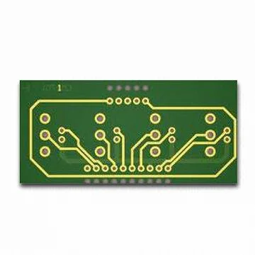
| Min PAD (inner layer) | 5 mil(0.13mm) | hole ring width | |
| Min thickness(inner layer) | 4 mil(0.1mm) | without copper | |
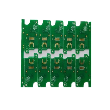
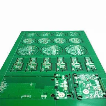
| Inner copper thickness | 1~4 oz | ||
| Outer copper thickness | 0.5~6 oz | ||
| Finished board thickness | 0.4-3.2 mm | ||
Board thickness tolerance control | ±0.10 mm | ±0.10 mm | 1~4 L |
| ±10% | ±10% | 6~8 L | |
| ±10% | ±10% | ≥10 L | |
| Inner layer treatment | brown oxidation | ||
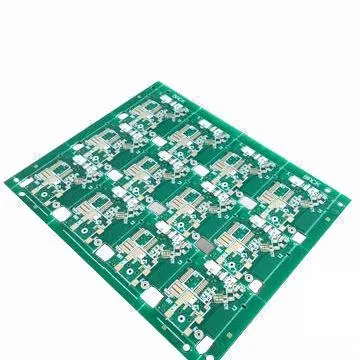
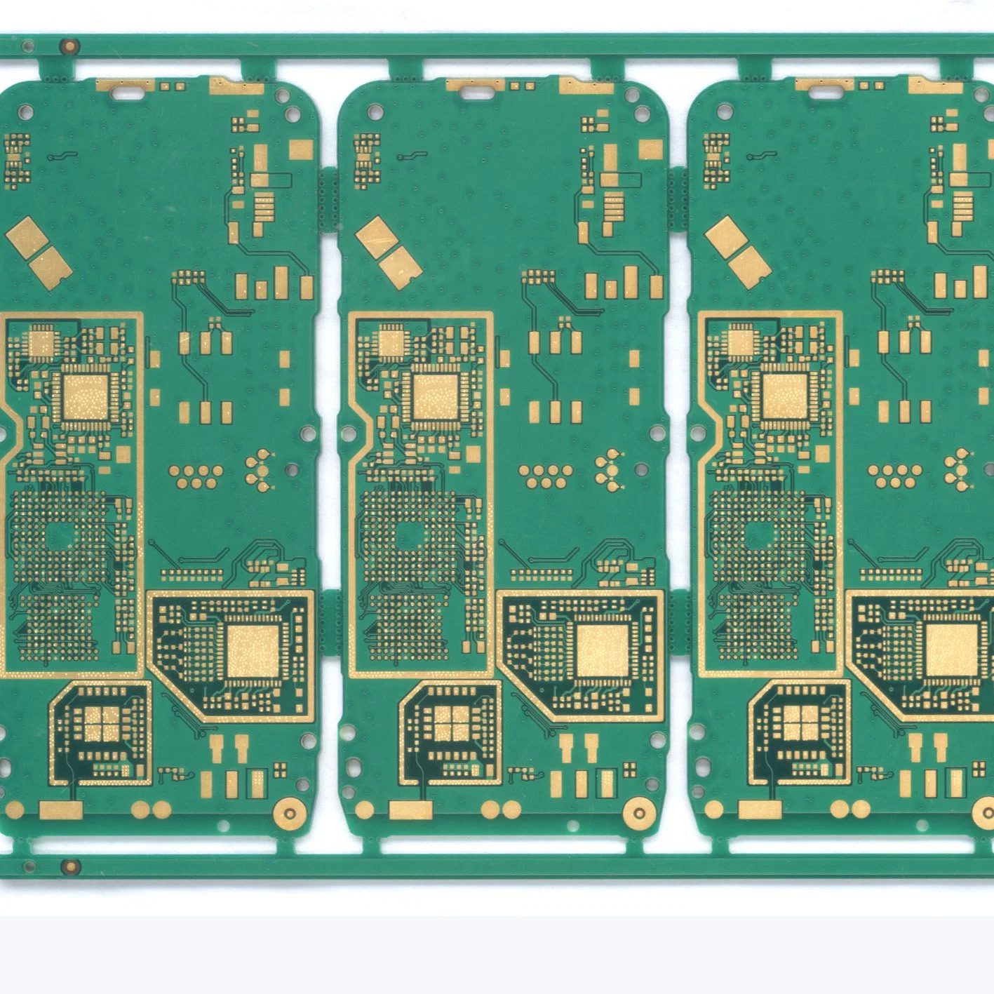
| Layer count Capability | 1-30 LAYER | ||
| alignment between ML | ±2mil | ||
| Min drilling | 0.15 mm | ||
| Min finished hole | 0.1 mm | ||
| Hole precision | ±2 mil(±50 um) | ||
| tolerance for Slot | ±3 mil(±75 um) | ||
| tolerance for PTH | ±3 mil(±75um) | ||
| tolerance for NPTH | ±2mil(±50um) | ||
| Max Aspect Ratio for PTH | 8:1 | ||
| Hole wall copper thickness | 15-50um | ||
| Alignment of outer layers | 4mil/4mil | ||
| Min trace width/space for outer layer | 4mil/4mil | ||
| Tolerance of Etching | +/-10% | ||
| Thickness of solder mask | on trace | 0.4-1.2mil(10-30um) | |
| at trace corner | ≥0.2mil(5um) | ||
| On base material | ≤+1.2mil Finished thickness | ||
| Hardness of solder mask | 6H | ||
| Alignment of solder mask film | ±2mil(+/-50um) | ||
| Min width of solder mask bridge | 4mil(100um) | ||
| Max hole with solder plug | 0.5mm | ||
| Surface finish | HAL (Lead or Lead free), immersion Gold, Immersion Nickel, Electric Gold finger, Electric Gold, OSP, Immersion Silver. | ||
| Max Nickel thickness for Gold finger | 280u"(7um) | ||
| Max gold thickness for Gold finger | 30u"(0.75um) | ||
| Nickel thickness in Immersion Gold | 120u"/240u"(3um/6um) | ||
| Gold thickness in Immersion Gold | 2u"/6u"(0.05um/0.15um) | ||
| Impedance control and its tolerance | 50±10%,75±10%,100±10% 110±10% | ||
| Trace Anti-stripped strength | ≥61B/in(≥107g/mm) | ||
| bow and twist | 0.75% | ||