PC28F128J3F75A IC NOR Flash Parallel 2.7V PROM

Min.Order: 10
Product origin: Shenzhen, Guangdong, China
Infringement complaint: complaintComplaint
US$ 0.79 ~ 1.12

Description

Description

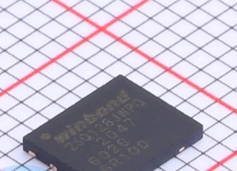
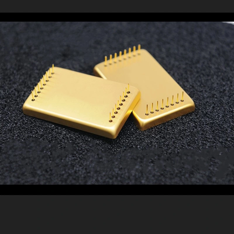
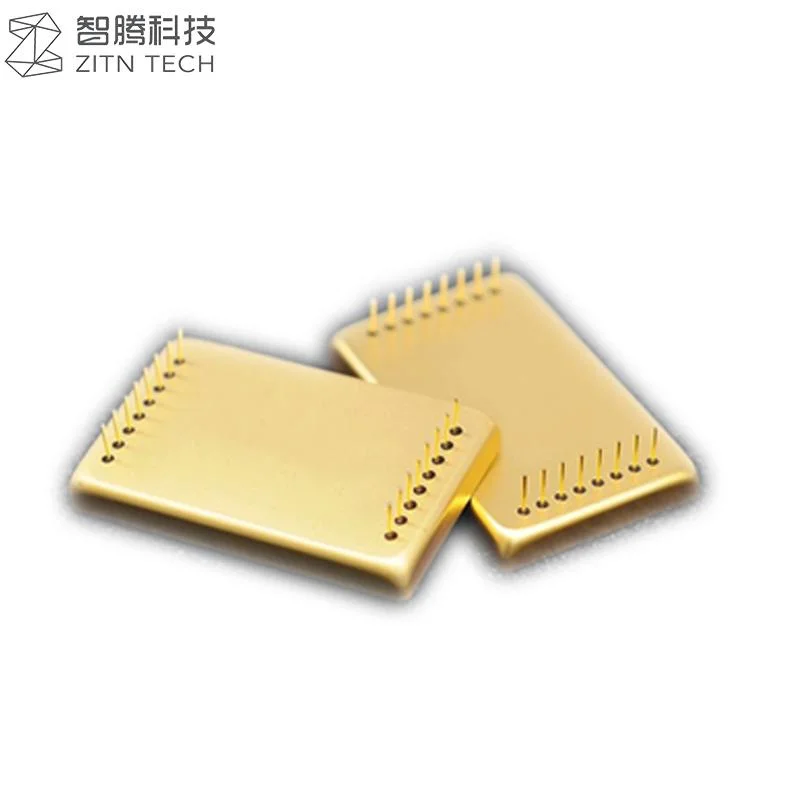
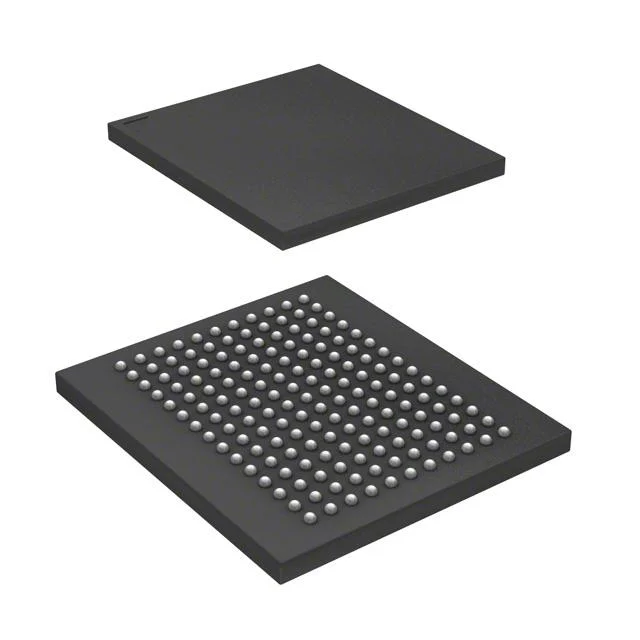
PC28F128J3F75A:  IC CHIPS

Package: BGA

Mfr. Part#: PC28F128J3F75A

Mfr.: MICRON

Datasheet: (e-mail or chat us for PDF file)

ROHS Status: 

Quality: 100% Original

Warranty: 180 days

Product Status
Active
 
Memory Type
Non-Volatile
 
Memory Format
FLASH
 
Technology
FLASH - NOR
 
Memory Size
128Mbit
 
Memory Organization
16M x 8, 8M x 16
 
Memory Interface
Parallel
 
Write Cycle Time - Word, Page
75ns
 
Access Time
75 ns
 
Voltage - Supply
2.7V ~ 3.6V
 
Operating Temperature
-40°C ~ 85°C (TA)
 
Mounting Type
Surface Mount
 
Package / Case
64-TBGA
 
Supplier Device Package
64-EasyBGA (10x13)
 
Base Product Number
PC28F128


The J3 65 nm SBC device provides improved mainstream performance with enhanced security features, taking advantage of the high quality and reliability of the NOR-based 65 nm technology. Offered in 128-Mbit, 64-Mbit, and 32-Mbit densities, the J3 65 nm SBC device brings reliable, low-voltage capability (3 V read, program, and erase) with high speed, low-power operation. The J3 65 nm SBC device takes advantage of proven manufacturing experience and is ideal for code and data applications where high density and low cost are required, such as in networking, telecommunications, digital set top boxes, audio recording, and digital imaging. Numonyx Flash Memory components also deliver a new generation of forward-compatible software support. By using the Common Flash Interface (CFI) and Scalable Command Set (SCS), customers can take advantage of density upgrades and optimized write capabilities of future Numonyx Flash Memory devices.

Key Features

  • Architecture
    • Symmetrical 128-KB blocks
    • 128 Mbit (128 blocks)
    • 64 Mbit (64 blocks)
    • 32 Mbit (32 blocks)
    • Blank Check to verify an erased block
  • Performance
    • Initial Access Speed: 75ns
    • 25 ns 8-word Asynchronous page-mode reads
    • 256-Word write buffer for x16 mode, 256- Byte write buffer for x8 mode; 1.41 μs per Byte Effective programming time
  • System Voltage
    • VCC = 2.7 V to 3.6 V
    • VCCQ = 2.7 V to 3.6 V
  • Packaging
    • 56-Lead TSOP
    • 64-Ball Easy BGA package
  • Security
    • Enhanced security options for code protection
    • Absolute protection with VPEN = Vss
    • Individual block locking
    • Block erase/program lockout during power transitions
    • Password Access feature
    • One-Time Programmable Register: 64 OTP bits, programmed with unique information by Numonyx 64 OTP bits, available for customer programming
  • Software
    • Program and erase suspend support
    • Numonyx® Flash Data Integrator (FDI)
    • Common Flash Interface (CFI) Compatible
    • Scalable Command Set
  • Quality and Reliability
    • Operating temperature: -40 °C to +85 °C
    • 100K Minimum erase cycles per block
    • 65 nm Flash Technology
    • JESD47E Compliant


Why choosing us

  • Located in Shenzhen, the electronic market center of China.
  • 100% guarantee components quality: Genuine Original.
  • Sufficient stock on your urgent demand.
  • Sophisticated colleagues help you solve problems to reduce your risk with on-demand manufacturing
  • Faster shipment: In stock components can ship the same day .
  • 24 Hours service 


Notice:

  1. Product images are for reference only.
  2. You can contact sales person to apply for a better price.
  3.  For more products, Pls do not hesitate to contact our Sales team.   
Product Tag:
Related categories:
Scroll to Top