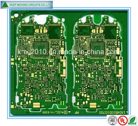
 Complaint

| No | Items | Production Capability |
| 1 | PCB Counts | 1 ~ 50 layers |
| 2 | Material Type | FR4,High TG , CEM1,CEM3,PTFE,Aluminum Base,Arlon,Rogers,Halogen free |
| 3 | Maximum Panel Size | 500mmx1200mm |
| 4 | Board Outline Tolerance | Routing:±0.13mm ;Punching:±0.05mm |
| 5 | Finished Board Thickness | 0.20mm--6.00mm |
| 6 | Finshed Board Thickness Tolerance | >=0.8mm : ±8% ; <0.8mm: ±10% |
| 7 | Minimum Trace Width/Space | 0.003" /0.003" |
| 8 | Finished Outer Copper Thickness | 1OZ---5OZ |
| 9 | Finshed Inner Cooper Thickness | 0.50OZ--5OZ |
| 10 | Finished Hole Size | 0.10mm--6.30mm |
| 11 | Hole Size Tolerance | NPTH: ±0.05mm ; PTH: ±0.076mm |
| 12 | Hole Location Registration(Mechanical) | ±0.08mm |
| 13 | Aspect Ratio | 13:01 |
| 14 | Solder Mask Type | LPI |
| 15 | SMT Mini.Solder Mask Width | 0.08mm |
| 16 | Plug Via Diameter | 0.25mm--0.60mm |
| 17 | Impedance Control Tolerance | ±5% |
| 18 | Surface Treatment Type | HASL;HASL+Lead Free;Immersion Gold;Immersion Tin;Flash Gold; OSP;Immersion Silver;Gold Finger;Carbon Ink;Peelable Mask |
| Feature | Laser via PCB capability | ||||||
| Mass production | Sample Run(Small Value) | ||||||
| (Normal lower cost) | (High Value normal) | (High Value higher cost) | |||||
| Line /space width (trace layers) | .005"/.005" | .004"/.004" | .003"/.003" | .0025" | |||
| Line /space width (HDI layers) | .005"/.005" | .004"/.004" | .003"/.003" | .0025" | |||
| Drill via size (PTH) | .010" | .010" | .010" | .008" | |||
| Drill capture pad (PTH) | .022" | .020" | .018" | .016" | |||
| Micro via size (unfinished) | RCC | .004" | .004" | .004" | . 003" | ||
| Micro capture pad | .014" | .012" | .011" | .009" | |||
| Micro via size (unfinished) | PP | .005" | .004" | .004" | .003" | ||
| Micro capture pad | .014" | .012" | .011" | .010" | |||
| Aspect ratio (PTH) | 8:01 | 9:01 | 10:01 | 11:01 | |||
| Aspect ratio (Micro via) | 0.6:1 | 0.8:1 | 0.9:1 | 1:01 | |||
| Layer to layer Registration | ±5mil | ±4mil | ±3mil | ±2mil | |||
| Impedance control | ±10%(±5Ω) | ±10%(±4Ω | ±7%(±3Ω) | ±5%(±2.5Ω) | |||
Our service
| Inquiry | 1. Please send the BOM list and PCB Gerber files to us for detail quotation |
| 2. If you need to design, please provide us the schematic, functions of product, size etc. Sample and Picture would be better. | |
| Quotation | 1. Engineer confirms PCB requirements and Purchasing department confirms components. |
| 2. Quotation will be offered within 3 working days. | |
| Payment | Regarding payment term: T/T, L/C. |
| Sample making | Few samples will be produced before full production; All steps are strictly performed by company control and quality control. |
| Mass Production | After sample confirmed discussion about packing, shipping. Production department start the order schedule. |
Our quality