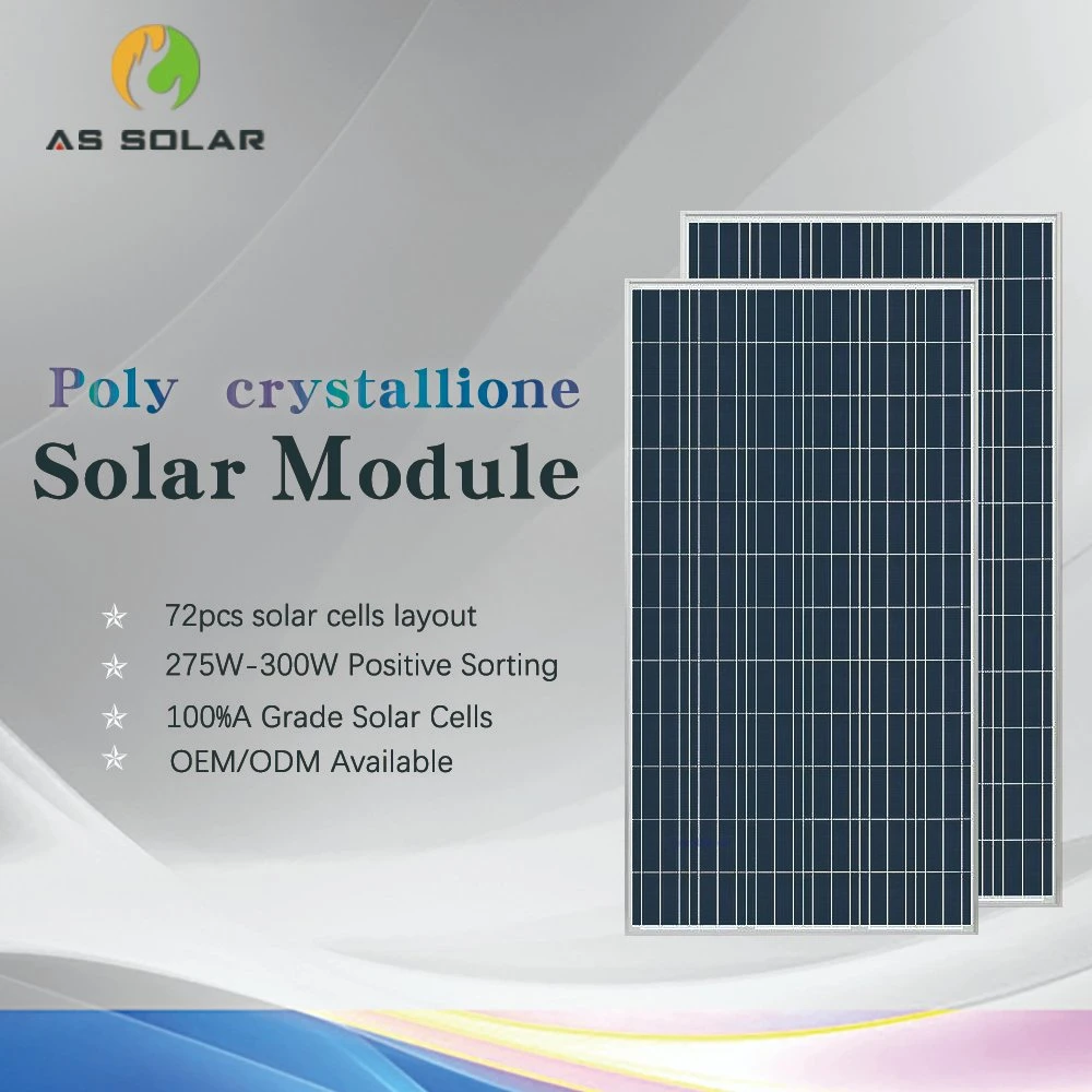
Description
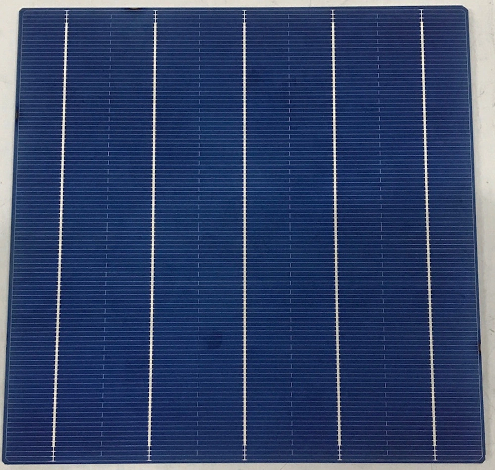
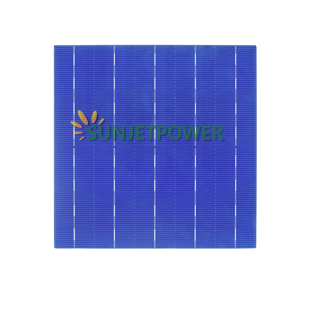
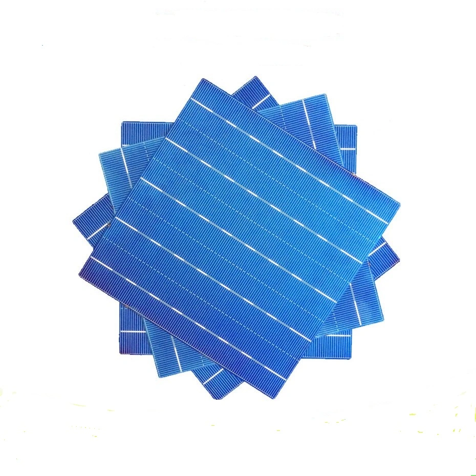
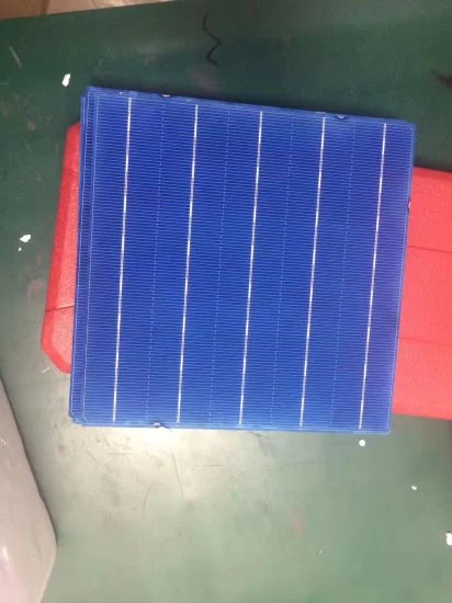
Physical characteristics:| Product | FLAGSUN 5BB 156*156mm Polycrystalline Silicon Solar Cell |
| Model Number | FSC-PP-025 |
| Material | Polycrystalline Silicon |
| Size | 156*156mm |
| Number of Cells | 1pcs |
| Efficiency | 17%~20% |
| Max. Power | 4.28~4.65watt |
| Thickness | 200 μm +/-20μm |
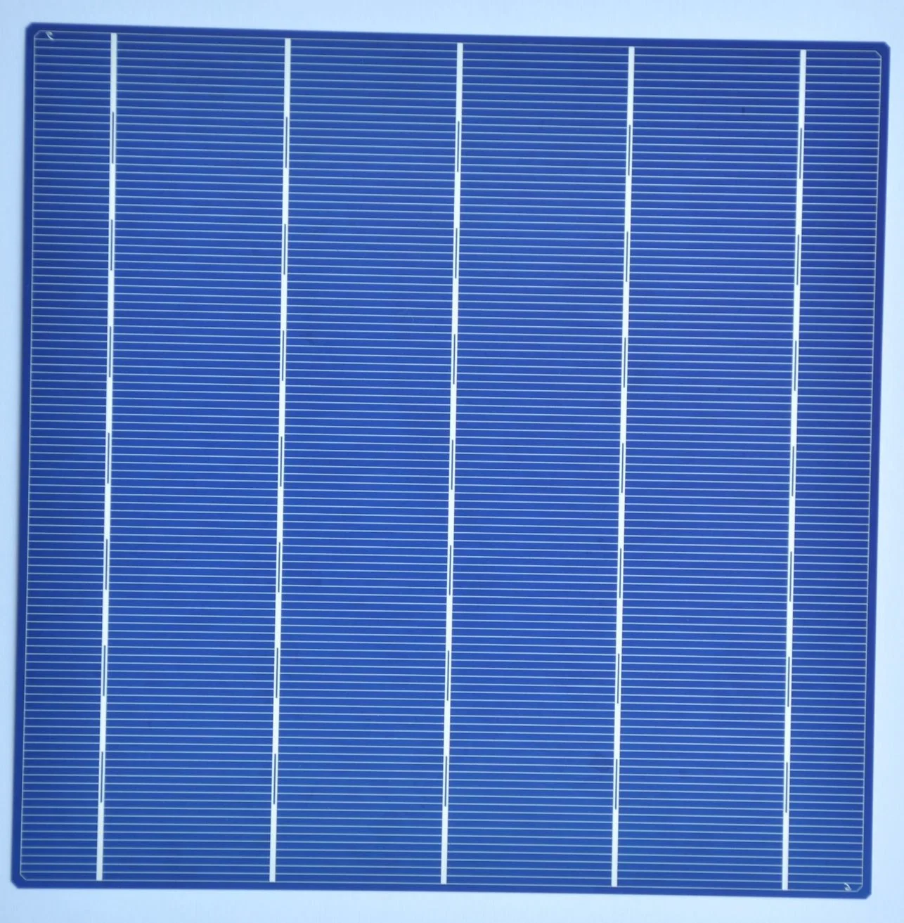
| Front | 1.0mm Bus Bars(Silver);Dark Blue Silicon Nitride AR Coating. |
| Back | 2.5mm Wide Soldering Pads(Silver);Back Surface Field (Aluminium) |
High efficientData under standard testing conditions(STC):1000W/Sq.M, AM1.5, 25ºC
| NO | Efficiency(%) | Pmpp(W) | Vmpp(V) | Impp(A) | Voc(V) | Isc(A) | FF(%) |
| 11 | 18.90-19.00 | 4.64 | 0.544 | 8.559 | 0.639 | 9.072 | 80.27 |
| 10 | 18.80-18.90 | 4.62 | 0.543 | 8.528 | 0.638 | 9.052 | 80.19 |
| 9 | 18.70-18.80 | 4.60 | 0.541 | 8.519 | 0.637 | 9.033 | 80.12 |
| 8 | 18.60-18.70 | 4.57 | 0.540 | 8.499 | 0.636 | 9.011 | 80.06 |
| 7 | 18.50-18.60 | 4.55 | 0.538 | 8.476 | 0.635 | 8.988 | 80.02 |
| 6 | 18.40-18.50 | 4.53 | 0.537 | 8.451 | 0.633 | 8.964 | 79.97 |
| 5 | 18.30-18.40 | 4.50 | 0.536 | 8.426 | 0.632 | 8.939 | 79.90 |
| 4 | 18.20-18.30 | 4.48 | 0.535 | 8.400 | 0.631 | 8.913 | 79.86 |
| 3 | 18.10-18.20 | 4.45 | 0.534 | 8.371 | 0.630 | 8.885 | 79.82 |
| 2 | 18.00-18.10 | 4.43 | 0.532 | 8.350 | 0.629 | 8.866 | 79.69 |
| 1 | 17.90-18.00 | 4.40 | 0.531 | 8.320 | 0.629 | 8.848 | 79.46 |
Flagsun's manufacturing covers the photovoltaic value chain from ingot casting and wafering through solar cell production and solar panel assembly.All the cell is with most strict quality standard in every production process .
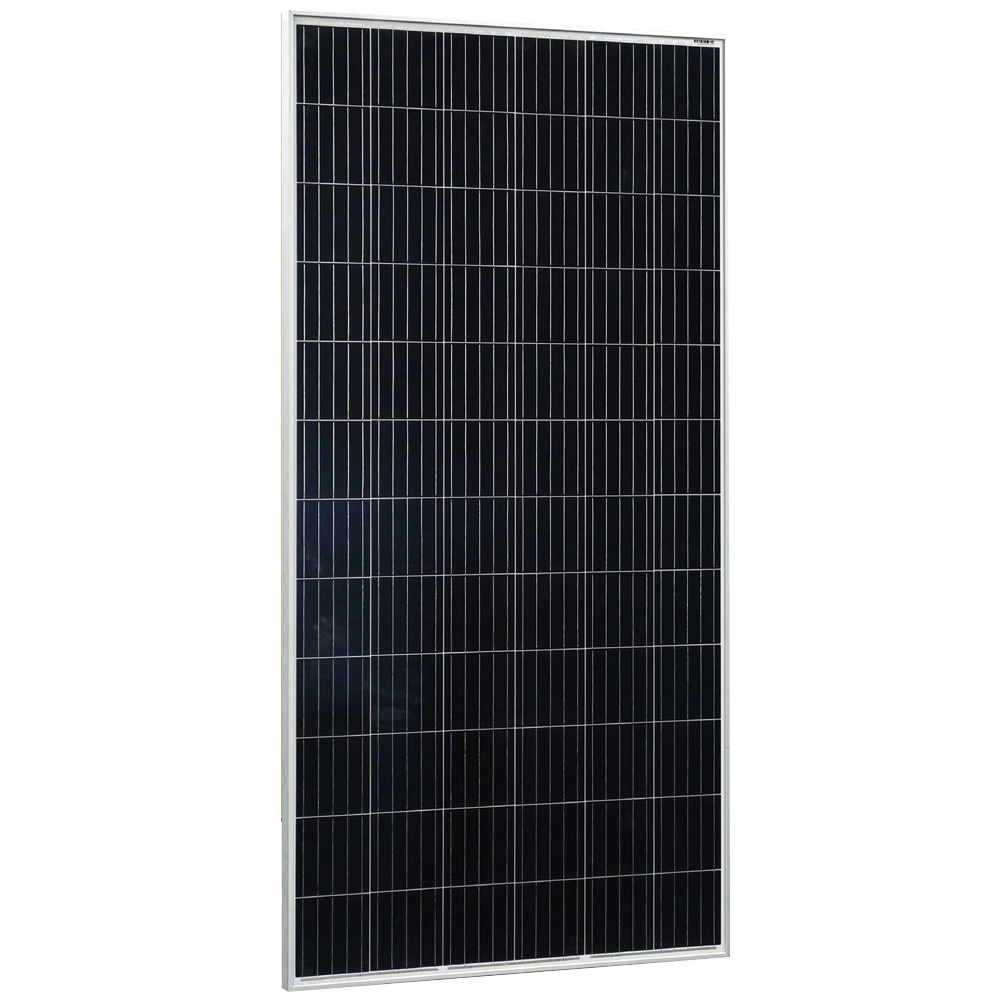
Product drawingFeatures:1.High conversion efficiency resulting in superior power output performance.
2.Outstanding power output even in low light or high temperature conditions
3.Optimized design for ease of soldering and lamination
4.Long-term stability,reliability and performance
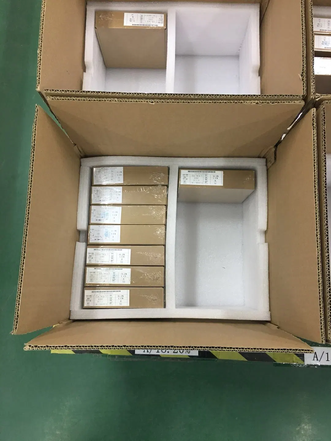
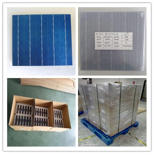
5.Output power tolerance of +/-3% Typical package for one box is 1200 cells. These cells are sealed in paper boards every 100 pcs.
Gross weight per unit shall be around 15 kg.
Solar Cell Production LineCleaning & Texturing: Wafers are cleaned with industrial soaps and form square-based pyramids also called texture. The texturization helps to reduce the reflection of sunlight.
Diffusion: Wafers that have been pre-droped with boron during the casting process are then given a negative(n-type) surface characteristic by diffusing them with a phosphorus source at high temperature, which in turn creats the negative/positive(n-p) junction.
Etching: Phosphorus diffuses not only into the desired wafer surface but also into the side and the opposite surface to form PN. This gives a shunt path between the cell front and rear. Removal of the path around the wafer edge/edge junction isolation is named etching.
PECVD: By PECVD equipment, the wafers are coated with anti-reflection coating(ARC). It's the blue silicion nitride film to reduce reflection and promote absorption of light.
Printing & Heating: it was adopted by printing paste with screen technology to print the electrodes of silicion solar, and form a good ohmic contact.
Testing & Sorting: It means classifying the cells according to their efficiency tested under the simulated sunlight.
Manufacture processCustom packaging
 Complaint