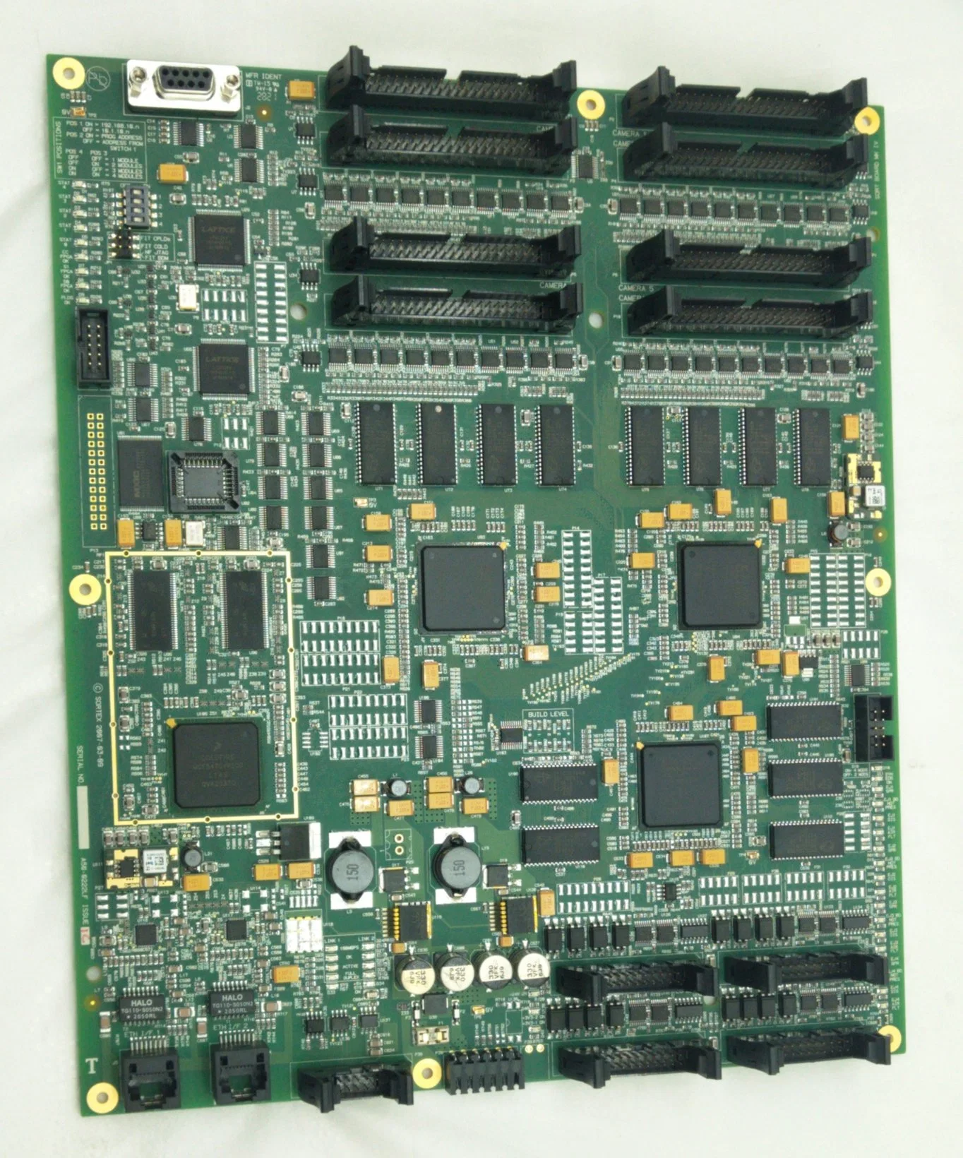
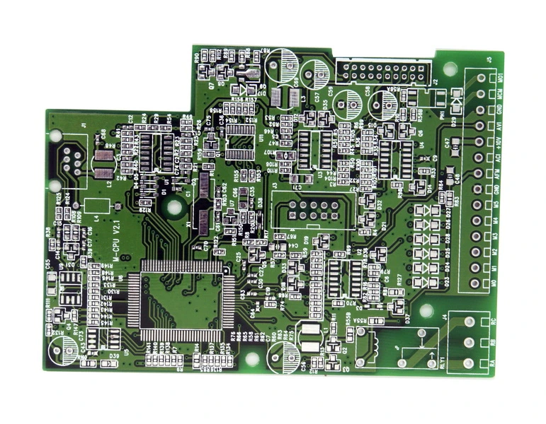
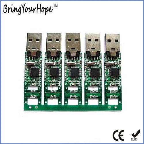
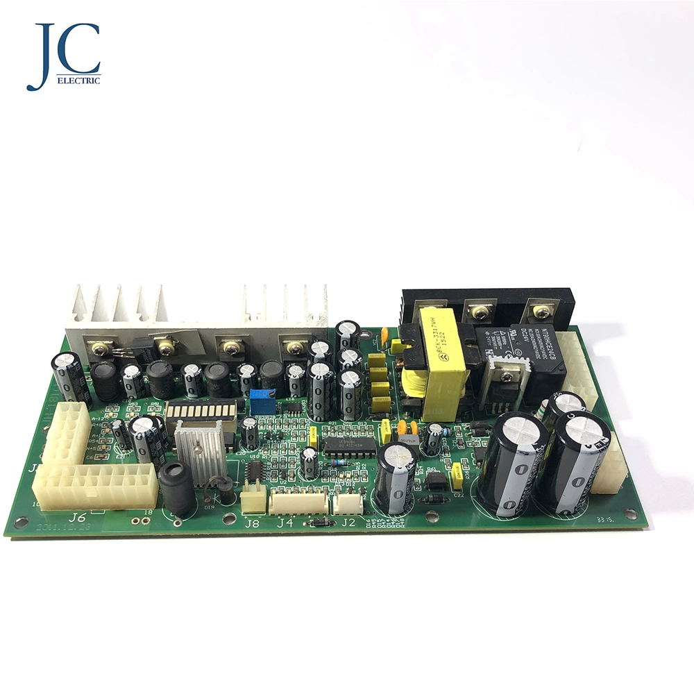
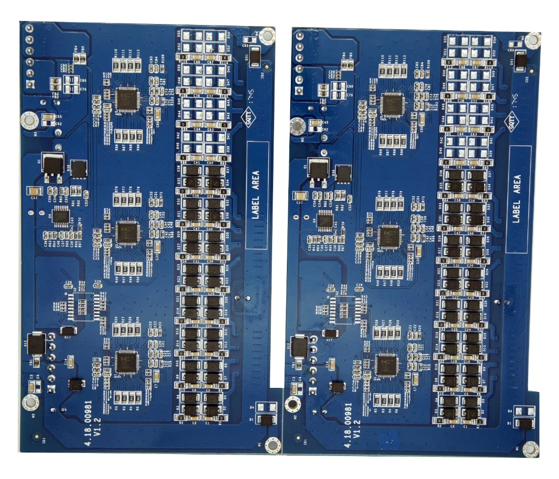
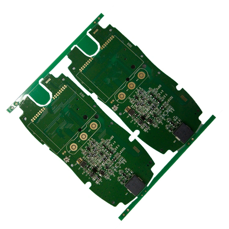
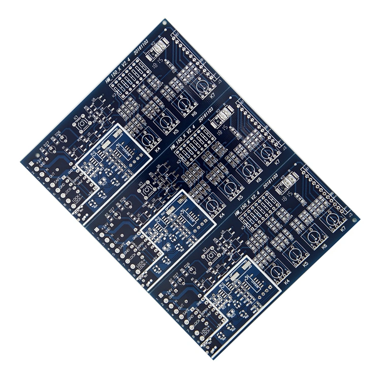
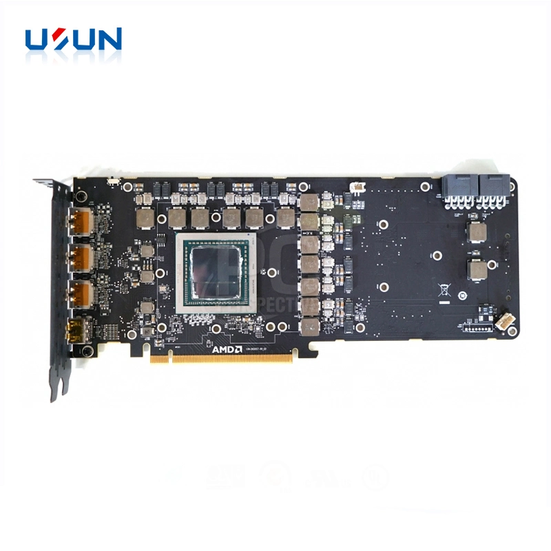
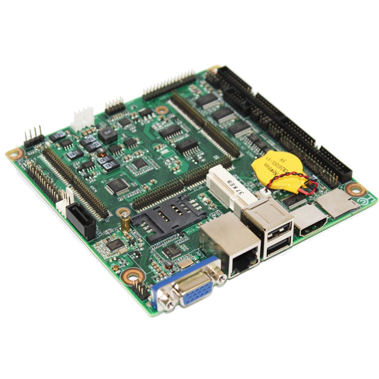
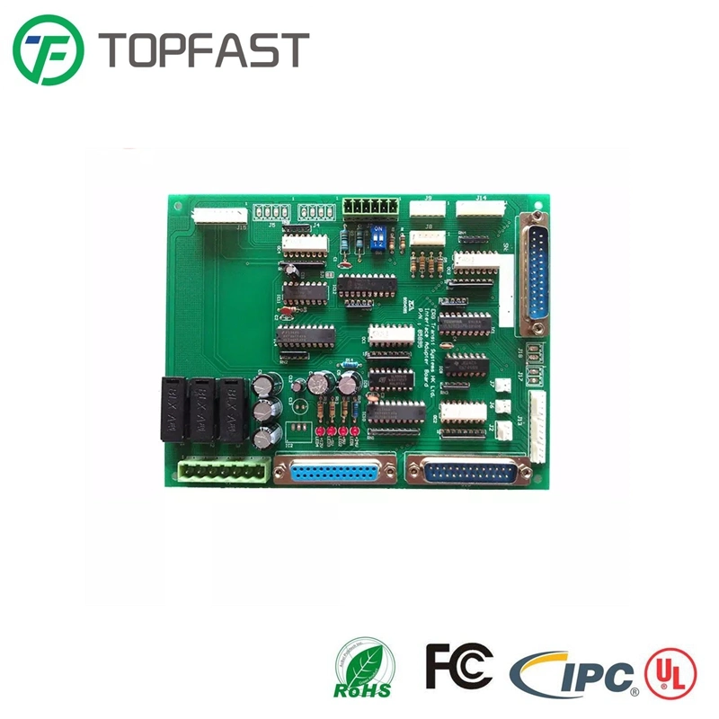
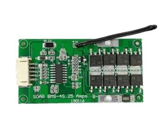
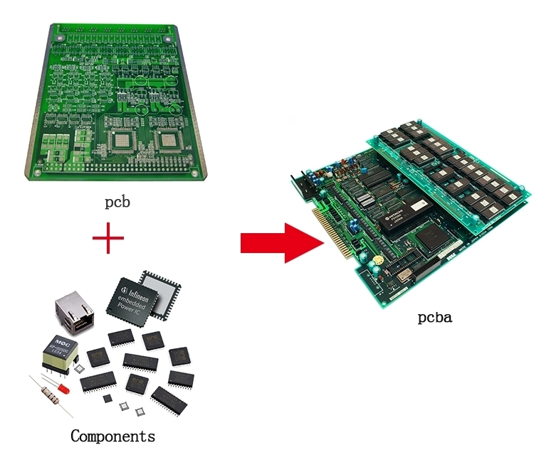
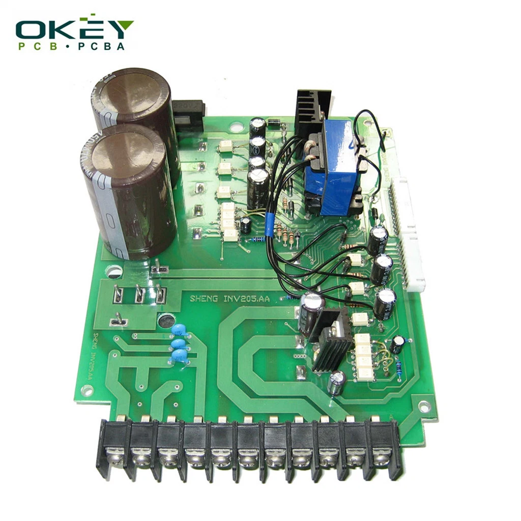
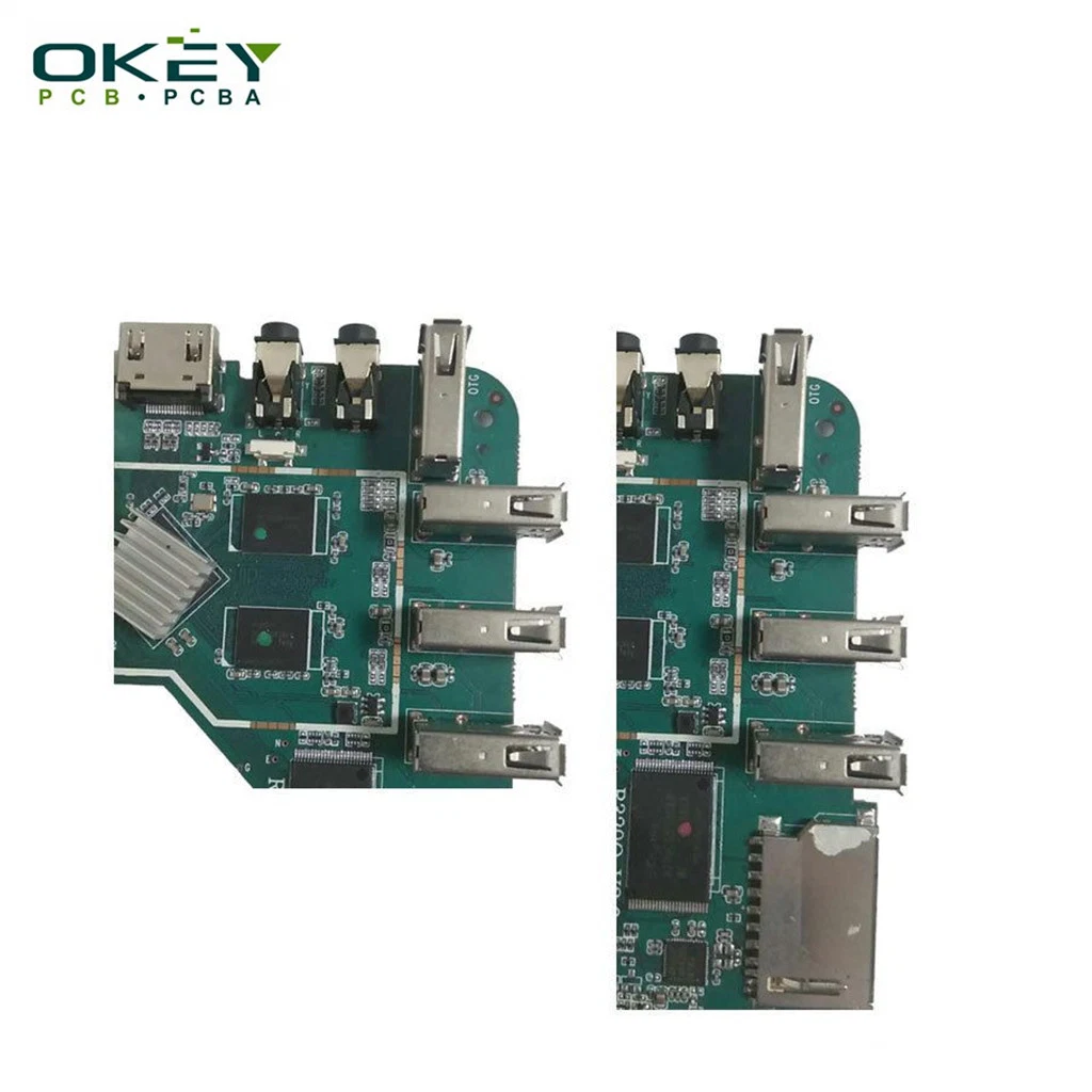
Description
Our Advantage:
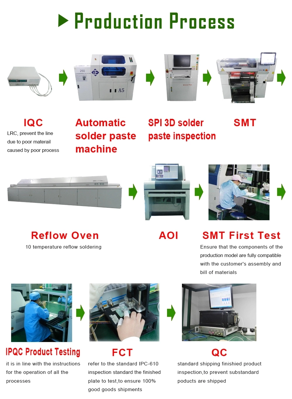
1. Free programming and free functional test, free package.
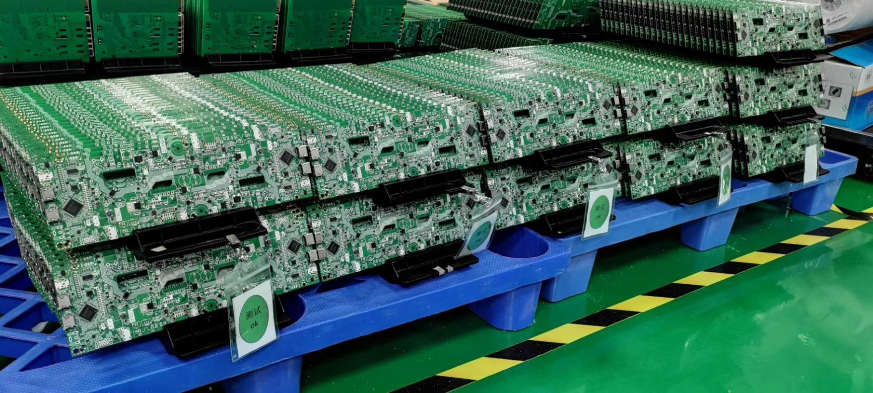
2. High quality: IPC-A-610E standard, E-test, X-ray, AOI test, QC, 100% funtional test.
3. Professional service. ISO SMT and through hole assembly, over 12 years experience.
4. Certification for electronics: UL, 94v-0, CE, SGS, FCC, RoHS, ISO9001:2008, ISO14001.
5. 24 hours online service.| Items | Speci. |
| Max panel size | 32" x 20.5"(800mm x 520mm) |
| Min trace width/ space (inner layer) | 4mil/4mil(0.1mm/0.1mm) |
| Min PAD (inner layer) | 5 mil(0.13mm) |
| Min thickness(inner layer) | 4 mil(0.1mm) |
| Inner copper thickness | 1~4 oz |
| Outer copper thickness | 0.5~6 oz |
| Finished board thickness | 0.4-3.2 mm |
| Board thickness tolerance control | ±0.10 mm | ±0.10 mm |
| ±10% | ±10% |
| ±10% | ±10% |
| Inner layer treatment | brown oxidation |
| Layer count Capability | 1-30 LAYER |
| alignment between ML | ±2mil |
| Min drilling | 0.15 mm |
| Min finished hole | 0.1 mm |
| Hole precision | ±2 mil(±50 um) |
| tolerance for Slot | ±3 mil(±75 um) |
| tolerance for PTH | ±3 mil(±75um) |
| tolerance for NPTH | ±2mil(±50um) |
| Max Aspect Ratio for PTH | 08:01 |
| Hole wall copper thickness | 15-50um |
| Alignment of outer layers | 4mil/4mil |
| Min trace width/space for outer layer | 4mil/4mil |
| Tolerance of Etching | +/-10% |
| Thickness of solder mask | on trace | 0.4-1.2mil(10-30um) |
| at trace corner | ≥0.2mil(5um) |
| On base material | ≤+1.2mil |
| Finished thickness |
| Hardness of solder mask | 6H |
| Alignment of solder mask film | ±2mil(+/-50um) |
| Min width of solder mask bridge | 4mil(100um) |
| Max hole with solder plug | 0.5mm |
| Surface finish | HAL (Lead or Lead free), immersion Gold, Immersion Nickel, Electric Gold finger, Electric Gold, OSP, Immersion Silver. |
| Max Nickel thickness for Gold finger | 280u"(7um) |
| Max gold thickness for Gold finger | 30u"(0.75um) |
| Nickel thickness in Immersion Gold | 120u"/240u"(3um/6um) |
| Gold thickness in Immersion Gold | 2u"/6u"(0.05um/0.15um) |
| Impedance control and its tolerance | 50±10%,75±10%,100±10% 110±10% |
| Trace Anti-stripped strength | ≥61B/in(≥107g/mm) |
| bow and twist | 0.75% |
|
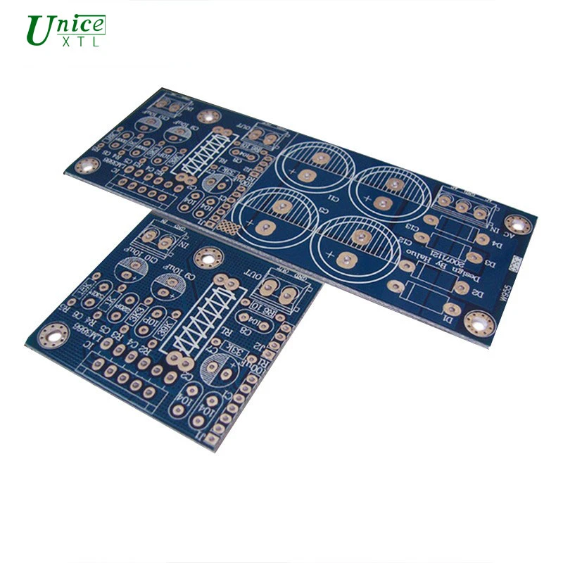
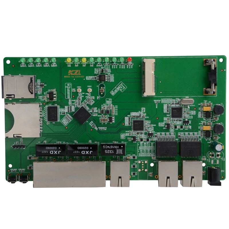
Double sided pcb board with osp finish:
Place of Origin Guangdong, China (Mainland)
Brand Name OKEY
Model Number okey pcb
Base Material FR-4
Copper Thickness 1 OZ
Board Thickness 1.2 mm
Min. Hole Size 0.4mm
Min. Line Width 0.2mm
Min. Line Spacing 0.15mm
Surface Finishing HASL
Color red
Small order acceptable
Fire resistanceUL-94V0
Outline/contourmilling, V-cut, CNC Routing
100% productsE-test or flying probe test
Features
Thin board capabilities
Increase routing density in complicated desig
Excellent mounting stability and reliability
Qualified material and surface treatment for Lead-free process
Applications
Smartphone, Feature Phone, Tablet, Ultrabook, e-Reader, MP3 Player, GPS, Portable Game Console, DSC, Camcorder, LCD Module
Benefits
Well experienced manufacturer with good yiel
Multiple plants increase production output in short time
| NO | Item | Technical capabilities |
| 1 | Layers | 1-20 layers |
| 2 | Max. Board size | 2000×610mm |
| 3 | Min. board Thickness | 2-layer 0.15mm |
| 4-layer 0.4mm |
| 6-layer 0.6mm |
| 8-layer 1.5mm |
| 10-layer 1.6~2.0mm |
| 4 | Min. line Width/Space | 0.1mm(4mil) |
| 5 | Max. Copper thickness | 10OZ |
| 6 | Min. S/M Pitch | 0.1mm(4mil) |
| 7 | Min. hole size | 0.2mm(8mil) |
| 8 | Hole dia. Tolerance (PTH) | ±0.05mm(2mil) |
| 9 | Hole dia. Tolerance (NPTH) | +0/-0.05mm(2mil) |
| 10 | Hole position deviation | ±0.05mm(2mil) |
| 11 | Outline tolerance | ±0.10mm(4mil) |
| 12 | Twist & Bent | 0.75% |
| 13 | Insulation Resistance | >10 12 Ω Normal |
| 14 | Electric strength | >1.3kv/mm |
| 15 | S/M abrasion | >6H |
| 16 | Thermal stress | 288°C 10Sec |
| 17 | Test Voltage | 50-300V |
| 18 | Min. blind/buried via | 0.15mm (6mil) |
| 19 | Surface Finished | HAL, ENIG, ImAg, Imsn OSP, Plating AG, Plating gold |
| 20 | Materials | FR4,H-TG,Teflon,Rogers,Ceramics,Aluminium, Copper base |
FAQQ1:What kind of PCB file format can you accept for production?
Gerber, PROTEL 99SE, PROTEL DXP, CAM350, ODB+(.TGZ)
Q2:Is my PCB files safe when I submit them to you for manufacturing?We respect customer's copyright and will never manufacture PCB for someone else with your files unless we receive written permission from you, nor we'll share these files with any other 3rd parties.NDA agreement is workable.Q3: Can you also handle PCB Assembly?We have our own PCB assembly factory which can help to source all the components for your product according to your BOM .Q4: Can you provide ODM and OEM service?We have experienced R&D team which can do research and design as your requests. Also we good at do reverse engineering .
Q5:What payments do you accept ?
-Wire Transfer(T/T),Western Union,Letter of Credit(L/C),Paypal ,Ali Pay,Credit Cart
Q6:How to ship the goods?
A:For small packages, we will ship the boards to you by DHL,UPS,FedEx,EMS. Door to door service! You will get your PCBs at your home.
B:For heavy goods more than 300kg, we may ship your boards by ship or by air to save freight cost. Of course, if you have your own forwarder,we may contact them for dealing with your shipment.
Q7:What is your minimum order quantity?
No MOQ limitation
Q8: Can we visit your company? No problem. You are welcome to visit us in Shenzhen. Or the other factory is in GuangDong province.
Q9: How can you ensure the quality of the PCBs?
Our PCBs and PCBA productions are 100% test including Flying Probe Test, E-test and AOI and functional test.
 Complaint