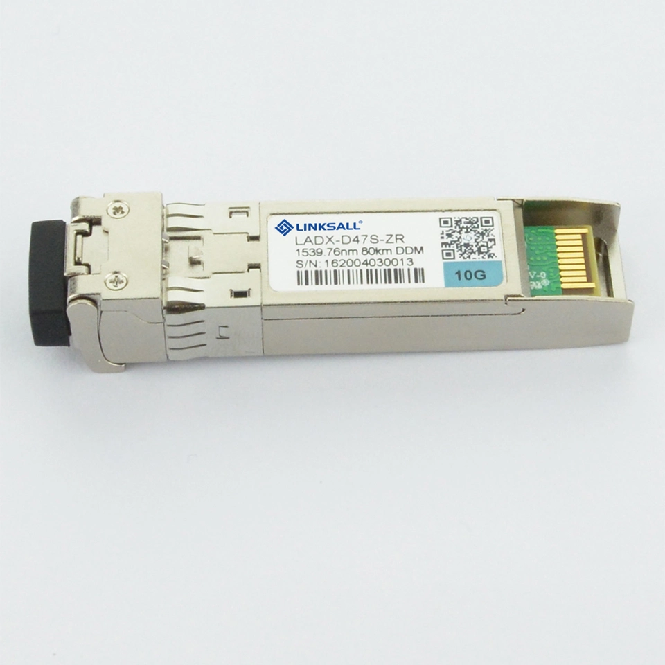


 Complaint

| Parameter | Symbol | Min. | Typ. | Max. | Unit | Note |
| Storage Temperature | Ts | -40 | - | +85 | ºC | |
| Relative Humidity | RH | 5 | - | 95 | % | |
| Power Supply Voltage | VCC | -0.3 | - | 4 | V | |
| Signal Input Voltage | Vcc-0.3 | - | Vcc+0.3 | V |
| Parameter | Symbol | Min. | Typ. | Max. | Unit | Note |
| Case Operating Temperature | TOP | 0 | - | +70 | ºC | Without air flow |
| Power Supply Voltage | VCC | 3.14 | 3.3 | 3.47 | V | |
| Power Supply Current | ICC | - | 450 | mA | ||
| Data Rate | BR | 10.3125 | 11.3 | Gbps | ||
| Transmission Distance | TD | - | 80 | km | ||
| Coupled fiber | Single mode fiber | 9/125um SMF | ||||
| Parameter | Symbol | Min. | Typical | Max. | Unit | Note |
| Supply Voltage | Vcc | 3.135 | 3.465 | V | ||
| Supply Current | Icc | 450 | mA | |||
| Power Consumption | P | 1.5 | W | |||
| Transmitter | ||||||
| Input differential impedance | Rin | 100 | Ω | 1 | ||
| Tx Input Single Ended DC Voltage Tolerance (Ref VeeT) | V | -0.3 | 4 | V | ||
| Differential input voltage swing | Vin,pp | 180 | 700 | mV | 2 | |
| Transmit Disable Voltage | VD | 2 | Vcc | V | 3 | |
| Transmit Enable Voltage | VEN | Vee | Vee+0.8 | V | ||
| Receiver | ||||||
| Single Ended Output Voltage Tolerance | V | -0.3 | 4 | V | ||
| Rx Output Diff Voltage | Vo | 300 | 850 | mV | ||
| Rx Output Rise and Fall Time | Tr/Tf | 30 | ps | 4 | ||
| LOS Fault | VLOS fault | 2 | VccHOST | V | 5 | |
| LOS Normal | VLOS norm | Vee | Vee+0.8 | V | 5 | |
| Parameter | Symbol | Min. | Typical | Max. | Unit | Note |
| Transmitter | ||||||
| Optical Wavelength-End Of Life | λ | X-100 | X | X+100 | pm | |
| Optical Wavelength-Beginning Of Life | λ | X-25 | X | X+25 | pm | |
| Average Optical Power | Pavg | 0 | +5 | dBm | 1 | |
| Laser Off Power | Poff | -30 | dBm | |||
| Extinction Ratio | ER | 8.2 | dB | |||
| Transmitter Dispersion Penalty | TDP | 3.0 | dB | 2 | ||
| Relative Intensity Noise | Rin | -128 | dB/Hz | 3 | ||
| Optical Return Loss Tolerance | 20 | dB | ||||
| Receiver | ||||||
| Center Wavelength | λr | 1480 | 1565 | nm | ||
| Receiver Sensitivity (OMA) | Sen | -23 | dBm | 4 | ||
| Stressed Sensitivity (OMA) | SenST | -21 | dBm | 4 | ||
| Los Assert | LOSA | -40 | - | dBm | ||
| Los Dessert | LOSD | -24 | dBm | |||
| Los Hysteresis | LOSH | 0.5 | dB | |||
| Overload | Sat | -7 | dBm | 5 | ||
| Receiver Reflectance | Rrx | -12 | dB | |||
| Parameter | Symbol | Min. | Typical | Max. | Unit |
| TX_Disable Assert Time | t_off | 10 | us | ||
| TX_Disable Negate Time | t_on | 1 | ms | ||
| Time to Initialize Include Reset of TX_FAULT | t_int | 300 | ms | ||
| TX_FAULT from Fault to Assertion | t_fault | 100 | us | ||
| TX_Disable Time to Start Reset | t_reset | 10 | us | ||
| Receiver Loss of Signal Assert Time | TA,RX_LOS | 100 | us | ||
| Receiver Loss of Signal Deassert Time | Td,RX_LOS | 100 | us | ||
| Rate-Select change Time | t_ratesel | 10 | us | ||
| Serial ID Clock Time | t_serial-clock | 100 | kHz |
| 0 | Symbol | Name/Description | Ref. |
| 1 | VEET | Transmitter Ground (Common with Receiver Ground) | 1 |
| 2 | TFAULT | Transmitter Fault. | 2 |
| 3 | TDIS | Transmitter Disable. Laser output disabled on high or open. | 3 |
| 4 | SDA | 2-wire Serial Interface Data Line | 4 |
| 5 | SCL | 2-wire Serial Interface Clock Line | 4 |
| 6 | MOD_ABS | Module Absent. Grounded within the module | 4 |
| 7 | RS0 | RS0 for Rate Select: Open or Low = Module supports 1.25 Gb/s High = Module supports 9.95 Gb/s to 10.3125 Gb/s | 5 |
| 8 | LOS | Loss of Signal indication. Logic 0 indicates normal operation. | 6 |
| 9 | RS1 | No connection required | 1 |
| 10 | VEER | Receiver Ground (Common with Transmitter Ground) | 1 |
| 11 | VEER | Receiver Ground (Common with Transmitter Ground) | 1 |
| 12 | RD- | Receiver Inverted DATA out. AC Coupled | |
| 13 | RD+ | Receiver Non-inverted DATA out. AC Coupled | |
| 14 | VEER | Receiver Ground (Common with Transmitter Ground) | 1 |
| 15 | VCCR | Receiver Power Supply | |
| 16 | VCCT | Transmitter Power Supply | |
| 17 | VEET | Transmitter Ground (Common with Receiver Ground) | 1 |
| 18 | TD+ | Transmitter Non-Inverted DATA in. AC Coupled. | |
| 19 | TD- | Transmitter Inverted DATA in. AC Coupled. | |
| 20 | VEET | Transmitter Ground (Common with Receiver Ground) | 1 |
| Data Address | Length (Byte) | Name of Length | Description and Contents |
| Base ID Fields | |||
| 0 | 1 | Identifier | Type of Serial transceiver (03h=SFP) |
| 1 | 1 | Reserved | Extended identifier of type serial transceiver (04h) |
| 2 | 1 | Connector | Code of optical connector type (07=LC) |
| 3-10 | 8 | Transceiver | 10G Base-XX |
| 11 | 1 | Encoding | 64B/66B |
| 12 | 1 | BR, Nominal | Nominal baud rate, unit of 100Mbps |
| 13-14 | 2 | Reserved | (0000h) |
| 15 | 1 | Length(9um) | Link length supported for 9/125um fiber, units of 100m |
| 16 | 1 | Length(50um) | Link length supported for 50/125um fiber, units of 10m |
| 17 | 1 | Length(62.5um) | Link length supported for 62.5/125um fiber, units of 10m |
| 18 | 1 | Length(Copper) | Link length supported for copper, units of meters |
| 19 | 1 | Reserved | |
| 20-35 | 16 | Vendor Name | SFP+ vendor name |
| 36 | 1 | Reserved | |
| 37-39 | 3 | Vendor OUI | SFP+ transceiver vendor OUI ID |
| 40-55 | 16 | Vendor PN | Part Number |
| 56-59 | 4 | Vendor rev | Revision level for part number |
| 60-62 | 3 | Reserved | |
| 63 | 1 | CCID | Least significant byte of sum of data in address 0-62 |
| Extended ID Fields | |||
| 64-65 | 2 | Option | Indicates which optical SFP signals are implemented(001Ah = LOS, TX_FAULT, TX_DISABLE all supported) |
| 66 | 1 | BR, max | Upper bit rate margin, units of % |
| 67 | 1 | BR, min | Lower bit rate margin, units of % |
| 68-83 | 16 | Vendor SN | Serial number (ASCII) |
| 84-91 | 8 | Date code | Manufacturing date code |
| 92-94 | 3 | Reserved | |
| 95 | 1 | CCEX | Check code for the extended ID Fields (addresses 64 to 94) |
| Vendor Specific ID Fields | |||
| 96-127 | 32 | Readable | specific date, read only |
| 128-255 | 128 | Reserved | Reserved for SFF-8079 |
| Data Address | Parameter | Accuracy | Unit |
| 96-97 | Transceiver Internal Temperature | ±3.0 | °C |
| 98-99 | VCC3 Internal Supply Voltage | ±3.0 | % |
| 100-101 | Laser Bias Current | ±10 | % |
| 102-103 | Tx Output Power | ±3.0 | dB |
| 104-105 | Rx Input Power | ±3.0 | dB |
| Feature | Reference | Performance |
| Electrostatic discharge(ESD) | IEC/EN 61000-4-2 | Compatible with standards |
| Electromagnetic Interference (EMI) | FCC Part 15 Class B EN 55022 Class B (CISPR 22A) | Compatible with standards |
| Laser Eye Safety | FDA 21CFR 1040.10, 1040.11 IEC/EN 60825-1,2 | Class 1 laser product |
| Component Recognition | IEC/EN 60950 ,UL | Compatible with standards |
| ROHS | 2002/95/EC | Compatible with standards |
| EMC | EN61000-3 | Compatible with standards |