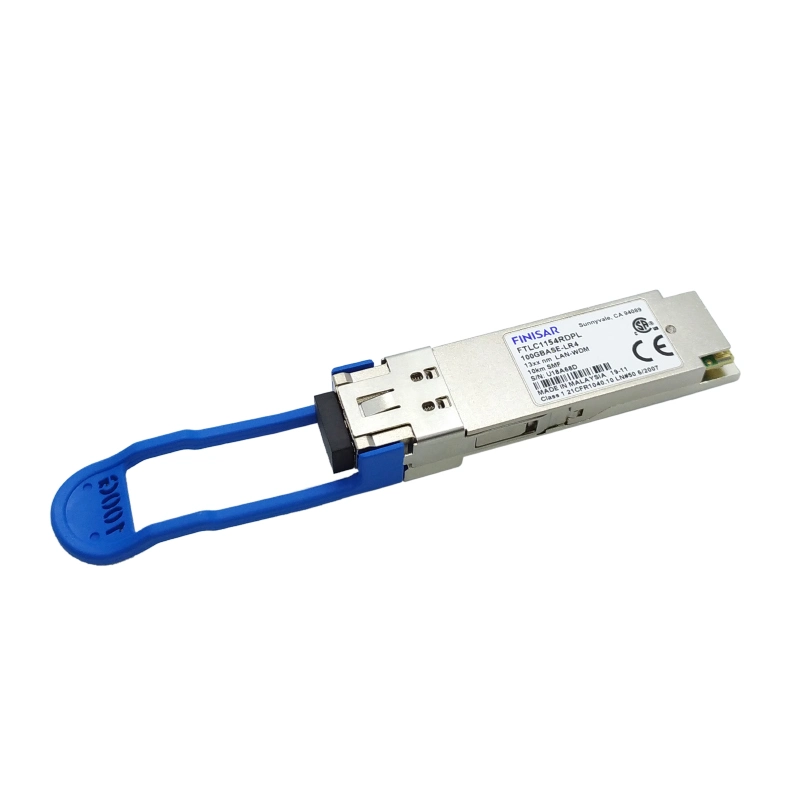
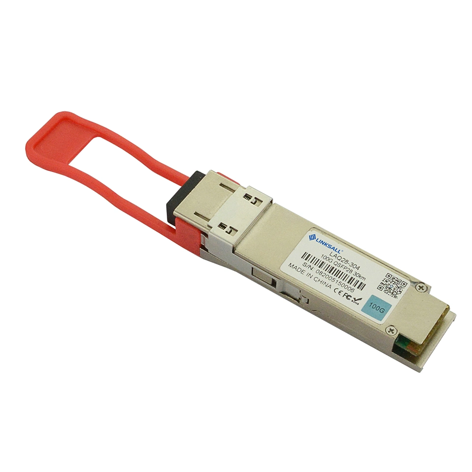
Generic Compatible 100gbase-Lr4 Qsfp28 1310nm 10km Dom Optical Transceiver Module

Min.Order: 1
Product origin: Shenzhen, Guangdong, China
Infringement complaint: complaintComplaint
US$ 1 ~ 265

Description

100Gb/s QSFP28 LR4 10km Transceiver

PRODUCT FEATURES 
  1. Compliant with 100GBASE-LR4
  2. Support line rates from 103.125 Gbps to 111.81 Gbps
  3. Integrated LAN WDM TOSA / ROSA for up to 10 km reach over SMF
  4. Digital Diagnostics Monitoring Interface
  5. Duplex LC optical receptacle
  6. No external reference clock
  7. Electrically hot-pluggable
  8. Compliant with QSFP28 MSA with LC connector
  9. Case operating temperature range:0°C to 70°C 
  10. Power dissipation < 3.5 W
 APPLICATIONS
  1. 100G Ethernet &100GBASE-LR4
  2. ITU-T OTU4
STANDARD
  1. Compliant to IEEE 802.3ba, IEEE 802.3bm and 100G LR4
  2. Compliant to SFF-8436
General Description
LAQ2-8429-LR optical Transceiver integrates receiver and transmitter path on one module. In the transmit side, four lanes of serial data streams are recovered, retimed, and passed to four laser drivers. The laser drivers control 4 Distributed Feedback Laser (DFB) with center wavelength of 1296 nm, 1300nm, 1305nm and 1309 nm. The optical signals are multiplexed to a single -mode fiber through an industry standard LC connector. In the receive side, the four lanes of optical data streams are optically de-multiplexed by the integrated optical de-multiplexer. Each data stream is recovered by a PIN photo-detector and trans-impedance amplifier, retimed. This module features a hot-pluggable electrical interface, low power consumption and MDIO management interface.
The product is designed with form factor, optical/electrical connection and digital diagnostic interface according to the QSFP28 Multi-Source Agreement (MSA) and compliant to IEEE 802.3bm.
Absolute Maximum Ratings 
ParameterSymbolMin.Typ.Max.UnitNote
Storage TemperatureTs-40-85ºC 
Relative HumidityRH5-95% 
Power Supply VoltageVCC-0.3-4V 
Signal Input Voltage Vcc-0.3-Vcc+0.3V 

Recommended Operating Conditions
ParameterSymbolMin.Typ.Max.UnitNote
Case Operating TemperatureTcase0-70ºCWithout air flow
Power Supply VoltageVCC3.133.33.47V 
Power Supply CurrentICC- 1060mA 
Data RateBR 25.78125 GbpsEach channel
Transmission DistanceTD -10km 
Coupled fiberSingle mode fiber9/125um SMF
Optical Characteristics
ParameterSymbolMinTypMaxUnitNOTE
Transmitter      
Wavelength Assignmentλ01294.531295.561296.59nm 
λ11299.021300.051301.09nm 
λ21303.541304.581305.63nm 
λ31308.091309.141310.19nm 
Total Output. PowerPOUT  10.5dBm 
Average Launch Power Per lane -4.3 4.5dBm 
Spectral Width (-20dB)σ  1nm 
SMSR 30  dB 
Optical Extinction RatioER4  dB 
Average launch Power off per lanePoff  -30dBm 
RINRIN  -128dB/Hz 
Output Eye Mask definition
{X1,X2,X3,Y1,Y2,Y3}
{0.25,0.4,0.45,0.25,0.28,0.4} 
Receiver      
Rx Sensitivity per laneRSENS  -10.6dBm1
LOS De-Assert LOSD -30  dBm 
LOS Assert LOSA   -12dBm 
Input Saturation Power (Overload)Psat  4.5dBm 
Receiver Reflectance Rr  -26dB 
Notes
  1. Measured with a PRBS 231-1 test pattern, @25.78Gb/s, BER<10-12
 
    1. Electrical Characteristics
ParameterSymbolMinTypMaxUnitNOTE
Supply VoltageVcc3.133.33.47V 
Supply CurrentIcc  1060mA 
Transmitter      
Input differential impedanceRin 100 Ω1
 Differential data input swingVin,pp180 1000mV 
Transmit Disable VoltageVDVcc-1.3 VccV 
Transmit Enable VoltageVENVee Vee+ 0.8V2
Receiver      
Differential data output swingVout,pp300 850mV3
LOS FaultVLOS faultVcc-1.3 VccHOSTV4
LOS NormalVLOS normVee Vee+0.8V4
Notes
  1. Connected directly to TX data input pins. AC coupled thereafter. 
  2. Or open circuit. 
  3. Into 100 ohms differential termination. 
  4. Loss Of Signal is LVTTL. Logic 0 indicates normal operation; logic 1 indicates no signal detected. 
 
    1. Pin Assignment
Figure 1---Pin out of Connector Block on Host Board
PinSymbolName/DescriptionNOTE
1GNDTransmitter Ground  (Common with Receiver Ground)1
2Tx2nTransmitter Inverted Data Input 
3Tx2pTransmitter Non-Inverted Data output 
4GNDTransmitter Ground  (Common with Receiver Ground)1
5Tx4nTransmitter Inverted Data Input 
6Tx4pTransmitter Non-Inverted Data output 
7GNDTransmitter Ground  (Common with Receiver Ground)1
8ModSelLModule Select 
9ResetLModule Reset 
10VccRx3.3V Power Supply Receiver2
11SCL2-Wire serial Interface Clock 
12SDA2-Wire serial Interface Data 
13GNDTransmitter Ground  (Common with Receiver Ground) 
14Rx3pReceiver Non-Inverted Data Output  
15Rx3nReceiver Inverted Data Output 
16GNDTransmitter Ground  (Common with Receiver Ground)1
17Rx1pReceiver Non-Inverted Data Output 
18Rx1nReceiver Inverted Data Output 
19GNDTransmitter Ground  (Common with Receiver Ground)1
20GNDTransmitter Ground  (Common with Receiver Ground)1
21Rx2nReceiver Inverted Data Output 
22Rx2pReceiver Non-Inverted Data Output 
23GNDTransmitter Ground  (Common with Receiver Ground)1
24Rx4nReceiver Inverted Data Output1
25Rx4pReceiver Non-Inverted Data Output 
26GNDTransmitter Ground  (Common with Receiver Ground)1
27ModPrslModule Present 
28IntLInterrupt 
29VccTx3.3V power supply transmitter2
30Vcc13.3V power supply2
31LPModeLow Power Mode 
32GNDTransmitter Ground  (Common with Receiver Ground)1
33Tx3pTransmitter Non-Inverted Data Input 
34Tx3nTransmitter Inverted Data Output 
35GNDTransmitter Ground  (Common with Receiver Ground)1
36Tx1pTransmitter Non-Inverted Data Input 
37Tx1nTransmitter Inverted Data Output 
38GNDTransmitter Ground  (Common with Receiver Ground)1
Notes:
1. GND is the symbol for signal and supply (power) common for QSFP28 modules. All are common within the QSFP28 module and all module voltages are referenced to this potential unless otherwise noted. Connect these directly to the host board signal common ground plane.
2. VccRx, Vcc1 and VccTx are the receiving and transmission power suppliers and shall be applied concurrently. Recommended host board power supply filtering is shown below. Vcc Rx, Vcc1 and Vcc Tx may be internally connected within the QSFP28 transceiver module in any combination. The connector pins are each rated for a maximum current of 500mA.


    1. Digital Diagnostic Functions
     LAQ2-8429-LR support the 2-wire serial communication protocol as defined in the QSFP28 MSA. Which allows real-time access to the following operating parameters: 
  • Transceiver temperature 
  • Laser bias current 
  • Transmitted optical power
  • Received optical power
  • Transceiver supply voltage 
     It also provides a sophisticated system of alarm and warning flags, which may be used to alert end-users when particular operating parameters are outside of a factory-set normal range. 
     The operating and diagnostics information is monitored and reported by a Digital Diagnostics Transceiver Controller inside the transceiver, which is accessed through the 2-wire serial interface. When the serial protocol is activated, the serial clock signal (SCL pin) is generated by the host. The positive edge clocks data into the QSFP28 transceiver into those segments of its memory map that are not write-protected. The negative edge clocks data from the QSFP28 transceiver. The serial data signal (SDA pin) is bi-directional for serial data transfer. The host uses SDA in conjunction with SCL to mark the start and end of serial protocol activation. The memories are organized as a series of 8-bit data words that can be addressed individually or sequentially. The 2-wire serial interface provides sequential or random access to the 8 bit parameters, addressed from 00h to the maximum address of the memory.
     This clause defines the Memory Map for QSFP28 transceiver used for serial ID, digital monitoring and certain control functions. The interface is mandatory for all QSFP28 devices. The memory map has been changed in order to accommodate 4 optical channels and limit the required memory space. The structure of the memory is shown in Figure 2 -QSFP28 Memory Map. The memory space is arranged into a lower, single page, address space of 128 bytes and multiple upper address space pages. This structure permits timely access to addresses in the lower page, e.g. Interrupt Flags and Monitors. Less time critical entries, e.g. serial ID information and threshold settings, are available with the Page Select function. The structure also provides address expansion by adding additional upper pages as needed.  For example, in Figure 2 upper pages 01 and 02 are optional.  Upper page 01 allows implementation of Application Select Table, and upper page 02 provides user read/write space.  The lower page and upper pages 00 and 03 are always implemented. The interface address used is A0xh and is mainly used for time critical data like interrupt handling in order to enable a "one-time-read" for all data related to an interrupt situation. After an Interrupt, IntL, has been asserted, the host can read out the flag field to determine the effected channel and type of flag.
     For more detailed information including memory map definitions, please Contact our sales representatives.
 
 
Product Tag:
Related categories:
Scroll to Top