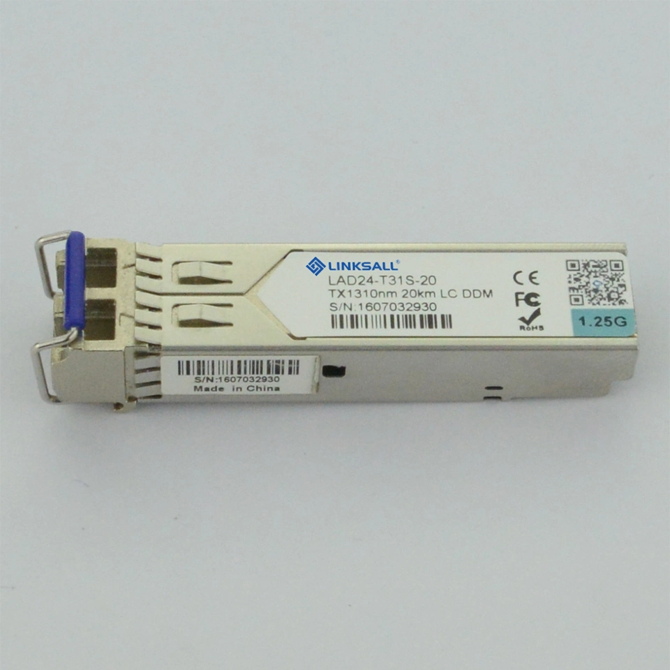
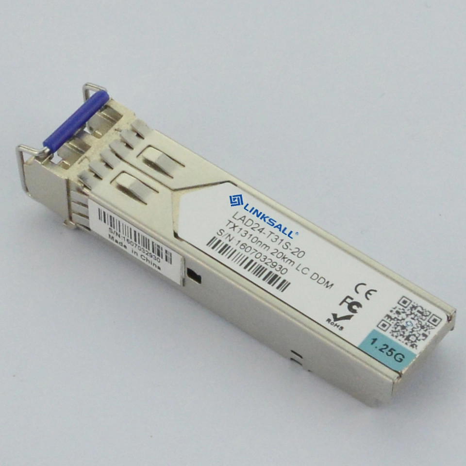
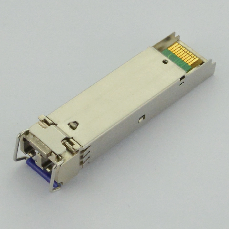

 Complaint

| Parameter | Symbol | Min. | Typical | Max. | Unit |
| Transmitter Differential Input Volt | +/-TX_DAT | 200 | 2400 | mV p-p | |
| Supply Current | ICC | 130 | 180 | mA | |
| Tx_Disable Input Voltage - Low | VIL | 0 | 0.8 | V | |
| Tx_Disable Input Voltage - High | VIH | 2.0 | Vcc | V | |
| Tx_Fault Output Voltage - Low | VOL | 0 | 0.8 | V | |
| Tx_Fault Output Voltage - High | VOH | 2.0 | Vcc | V | |
| Receiver Differential Output Volt | +/-RX_DAT | 600 | 1400 | mV p-p | |
| Rx_LOS Output Voltage- Low | VOL | 0 | 0.8 | V | |
| Rx_LOS Output Voltage- High | VOH | 2.0 | Vcc | V |
| Parameter | Symbol | Min. | Typical | Max. | Unit |
| Data Rate | B | - | 1250 | - | Mb/s |
| Centre Wavelength | λc | 1296 | 1310 | 1330 | nm |
| Output Spectral Width | △λ | - | - | 4 | nm |
| Average Output Power | Po | -9 | - | -3 | dBm |
| Extinction Ratio | EXT | 9 | - | - | dB |
| Data Input Voltage-High | VIHS | Vcc-1.16 | - | Vcc-0.89 | V |
| Data Input Voltage -Low | VILS | Vcc-1.82 | - | Vcc-1.48 | V |
| Supply Current | ICC | - | 90 | 150 | mA |
| Output Optical Eye | Compliant with IEEE802.3Z | ||||
| Receiver Section: | |||||
| Parameter | Symbol | Min. | Typical | Max. | Unit |
| Receive Sensitivity | Pmin | - | - | -25 | dBm |
| Maximum Input Power | PMAX | -3 | - | - | dBm |
| Signal Detect Threshold-De-Assert | SD | - | - | -23 | dBm |
| Signal Detect Threshold-Assert | SA | -33 | - | - | dBm |
| Hysteresis | - | - | 2.0 | - | dBm |
| Output High Voltage | VOH | Vcc-1.03 | - | Vcc-0.89 | V |
| Output Low Voltage | VOL | Vcc-1.82 | - | Vcc-1.63 | V |
| Operating Wavelength | λc | 1100 | - | 1600 | nm |
| Supply Current | ICC | - | 80 | 110 | mA |
| Parameter | Symbol | Remarks | Min. | Max. | Unit |
| Storage Temperature | TST | - | -40 | +85 | ºC |
| Operating Temperature | TIP | X=1 | 0 | +70 | ºC |
| X=2 | -40 | +85 | ºC | ||
| Input Voltage | TCC | - | 0 | +5 | V |
| Parameter | Symbol | Remarks | Min. | Typical | Max. | Unit | |
| Supply Voltage | VCC | - | +3.0 | +3.3 | +3.6 | V | |
| Operating Temperature | TOP | X=1 | 0 | - | +70 | ºC | |
| X=2 | -40 | - | +85 | ºC | |||
| Parameter | Symbol | Min. | Typical | Max. | Unit |
| TX_DISABLE Assert Time | t_off | 3 | 10 | usec | |
| TX_DISABLE Negate Time | t_on | 0.5 | 1 | msec | |
| Time to initialize include reset of TX_FAULT | t_int | 30 | 300 | msec | |
| TX_FAULT from fault to assertion | t_fault | 20 | 100 | usec | |
| TX_DISBEL time to start reset | t_reset | 10 | usec | ||
| Receiver Loss of Signal Assert Time (off to On) | TA,RX_LOS | 100 | usec | ||
| Receiver Loss of Signal Assert Time (on to off) | Td,RX_LOS | 100 | usec |
| Pin | Symbol | Name/Description | Ref |
| 1 | VEET | Transmitter Ground (Common with Receiver Ground) | 1 |
| 2 | TFAULT | Transmitter Fault. Low normal operation, High Fault indication | |
| 3 | TDIS | Transmitter Disable. Laser output disabled on high or open | 2 |
| 4 | MOD_DEF(2) | Module Definition 2.Data line for Serial ID | 3 |
| 5 | MOD_DEF(1) | Module Definition 1.Clock line for Serial ID | 3 |
| 6 | MOD_DEF(0) | Module Definition 0.Grounded within the moudle | 3 |
| 7 | Rate Select | No connection required | |
| 8 | LOS | Loss of Signal indication. Logic 0 indicates normal operation. | 4 |
| 9 | VEER | Receiver Ground (Common with Transmitter Ground) | 1 |
| 10 | VEER | Receiver Ground (Common with Transmitter Ground) | 1 |
| 11 | VEER | Receiver Ground (Common with Transmitter Ground) | 1 |
| 12 | RD- | Receiver Inverted DATA out.AC Coupled | |
| 13 | RD+ | Receiver Non-inverted DATA out.AC Coupled | |
| 14 | VEER | Receiver Ground (Common with Transmitter Ground) | 1 |
| 15 | VCCR | Receiver Power Supply | |
| 16 | VCCT | Transmitter Power Supply | |
| 17 | VEET | Transmitter Ground (Common with Receiver Ground) | 1 |
| 18 | TD+ | Transmitter Non-inverted DATA in.AC Coupled | |
| 19 | TD- | Transmitter Inverted DATA in.AC Coupled | |
| 20 | VEET | Transmitter Ground (Common with Receiver Ground) | 1 |
| Data Address | Length (Byte) | Name of Length | Description and Contents |
| Base ID Fields | |||
| 0 | 1 | Identifier | Type of Serial transceiver (03h=SFP) |
| 1 | 1 | Reserved | Extended identifier of type serial transceiver (04h) |
| 2 | 1 | Connector | Code of optical connector type (07=LC) |
| 3-10 | 8 | Transceiver | Gigabit Ethernet 1000Base-SX & Fiber Channel |
| 11 | 1 | Encoding | NRZ (03h) |
| 12 | 1 | BR,Nominal | Nominal baud rate, unit of 100Mbps |
| 13-14 | 2 | Reserved | (0000h) |
| 15 | 1 | Length(9um) | Link length supported for 9/125um fiber, units of 100m |
| 16 | 1 | Length(50um) | Link length supported for 50/125um fiber, units of 10m |
| 17 | 1 | Length(62.5um) | Link length supported for 62.5/125um fiber, units of 10m |
| 18 | 1 | Length(Copper) | Link length supported for copper, units of meters |
| 19 | 1 | Reserved | |
| 20-35 | 16 | Vendor Name | SFP vendor name |
| 36 | 1 | Reserved | |
| 37-39 | 3 | Vendor OUI | SFP transceiver vendor OUI ID |
| 40-55 | 16 | Vendor PN | Part Number: "LAS24-xxxxxx" (ASCII) |
| 56-59 | 4 | Vendor rev | Revision level for part number |
| 60-61 | 2 | Wavelength | Laser wavelength |
| 62 | 1 | Reserved | |
| 63 | 1 | CCID | Least significant byte of sum of data in address 0-62 |
| Extended ID Fields | |||
| 64-65 | 2 | Option | Indicates which optical SFP signals are implemented (001Ah = LOS, TX_FAULT, TX_DISABLE all supported) |
| 66 | 1 | BR, max | Upper bit rate margin, units of % |
| 67 | 1 | BR, min | Lower bit rate margin, units of % |
| 68-83 | 16 | Vendor SN | Serial number (ASCII) |
| 84-91 | 8 | Date code | Manufacturing date code |
| 92-94 | 3 | Reserved | |
| 95 | 1 | CCEX | Check code for the extended ID Fields (addresses 64 to 94) |
| Vendor Specific ID Fields | |||
| 96-127 | 32 | Readable | Specific date, read only |
| Address | Bytes | Name | Description |
| 00-01 | 2 | Temp High Alarm | MSB at low address |
| 02-03 | 2 | Temp Low Alarm | MSB at low address |
| 04-05 | 2 | Temp High Warning | MSB at low address |
| 06-07 | 2 | Temp Low Warning | MSB at low address |
| 08-09 | 2 | Voltage High Alarm | MSB at low address |
| 10-11 | 2 | Voltage Low Alarm | MSB at low address |
| 12-13 | 2 | Voltage High Warning | MSB at low address |
| 14-15 | 2 | Voltage Low Warning | MSB at low address |
| 16-17 | 2 | Bias High Alarm | MSB at low address |
| 18-19 | 2 | Bias Low Alarm | MSB at low address |
| 20-21 | 2 | Bias High Warning | MSB at low address |
| 22-23 | 2 | Bias Low Warning | MSB at low address |
| 24-25 | 2 | TX Power High Alarm | MSB at low address |
| 26-27 | 2 | TX Power Low Alarm | MSB at low address |
| 28-29 | 2 | TX Power High Warning | MSB at low address |
| 30-31 | 2 | TX Power Low Warning | MSB at low address |
| 32-33 | 2 | RX Power High Alarm | MSB at low address |
| 34-35 | 2 | RX Power Low Alarm | MSB at low address |
| 36-37 | 2 | RX Power High Warning | MSB at low address |
| 38-39 | 2 | RX Power Low Warning | MSB at low address |
| 40-55 | 16 | Reserved | Reserved for future monitored quantities |
| 56-59 | 4 | Rx_PWR(4) | Single precision floating point calibration data - Rx optical power. Bit 7 of byte 56 is MSB. Bit 0 of byte 59 is LSB. |
| 60-63 | 4 | Rx_PWR(3) | Single precision floating point calibration data - Rx optical power. Bit 7 of byte 60 is MSB. Bit 0 of byte 63 is LSB. |
| 64-67 | 4 | Rx_PWR(2) | Single precision floating point calibration data - Rx optical power. Bit 7 of byte 64 is MSB, bit 0 of byte 67 is LSB. |
| 68-71 | 4 | Rx_PWR(1) | Single precision floating point calibration data - Rx optical power. Bit 7 of byte 68 is MSB, bit 0 of byte 71 is LSB. |
| 72-75 | 4 | Rx_PWR(0) | Single precision floating point calibration data - Rx optical power. Bit 7 of byte 72 is MSB, bit 0 of byte 75 is LSB. |
| 76-77 | 2 | Tx_I(Slope) | Fixed decimal (unsigned) calibration data, laser bias current. Bit 7 of byte 76 is MSB, bit 0 of byte 77 is LSB. |
| 78-79 | 2 | Tx_I(Offset) | Fixed decimal (signed two's complement) calibration data, laser bias current. Bit 7 of byte 78 is MSB, bit 0 of byte 79 is LSB |
| 80-81 | 2 | Tx_PWR(Slope) | Fixed decimal (unsigned) calibration data, transmitter coupled output power. Bit 7 of byte 80 is MSB, bit 0 of byte81 is LSB. |
| 82-83 | 2 | Tx_PWR(Offset) | Fixed decimal (signed two's complement) calibration data, transmitter coupled output power. Bit 7 of byte 82 is MSB, bit 0 of byte 83 is LSB. |
| 84-85 | 2 | T(Slope) | Fixed decimal (unsigned) calibration data, internal module temperature. Bit 7 of byte 84 is MSB, bit 0 of byte 85 is LSB. |
| 86-87 | 2 | T(Offset) | Fixed decimal (signed two's complement) calibration data, internal module temperature. Bit 7 of byte 86 is MSB, bit 0 of byte 87 is LSB. |
| 88-89 | 2 | V(Slope) | Fixed decimal (unsigned) calibration data, internal module supply voltage. Bit 7 of byte 88 is MSB, bit 0 of byte 89 is LSB. |
| 90-91 | 2 | V(Offset) | Fixed decimal (signed two's complement) calibration data, internal module supply voltage. Bit 7 of byte 90 is MSB. Bit 0 of byte 91 is LSB. |
| 92-95 | 4 | Reserved | Reserved |
| Byte | Bit | Name | Description | |||
| Converted analog values. Calibrated 16 bit data | ||||||
| 96 | All | Temperature MSB | Internally measured module temperature. | |||
| 97 | All | Temperature LSB | ||||
| 98 | All | Vcc MSB | Internally measured supply voltage in transceiver. | |||
| 99 | All | Vcc LSB | ||||
| 100 | All | TX Bias MSB | Internally measured TX Bias Current. | |||
| 101 | All | TX Bias LSB | ||||
| 102 | All | TX Power MSB | Measured TX output power. | |||
| 103 | All | TX Power LSB | ||||
| 104 | All | RX Power MSB | Measured RX input power. | |||
| 105 | All | RX Power LSB | ||||
| 106 | All | Reserved MSB | Reserved for 1st future definition of digitized analog input | |||
| 107 | All | Reserved LSB | Reserved for 1st future definition of digitized analog input | |||
| 108 | All | Reserved MSB | Reserved for 2nd future definition of digitized analog input | |||
| 109 | All | Reserved LSB | Reserved for 2nd future definition of digitized analog input | |||
| Optional Status/Control Bits | ||||||
| 110 | 7 | TX Disable State | Digital state of the TX Disable Input Pin. Not supported. | |||
| 110 | 6 | Soft TX Disable | Read/write bit that allows software disable of laser.Not supported. | |||
| 110 | 5 | Reserved | ||||
| 110 | 4 | RX Rate Select State | Digital state of the SFP RX Rate Select Input Pin.Not supported. | |||
| 110 | 3 | Soft RX Rate Select | Read/write bit that allows software RX rate select.Not supported. | |||
| 110 | 2 | TX Fault | Digital state of the TX Fault Output Pin. | |||
| 110 | 1 | LOS | Digital state of the LOS Output Pin. | |||
| 110 | 0 | Data Ready | Indicates transceiver has achieved power up and data is ready | |||
| 111 | 7-0 | Reserved | Reserved. | |||
| Reserved Optional Alarm and Warning Flag Bits | ||||||
| 112 | 7 | Temp High Alarm | Set when internal temperature exceeds high alarm level. | |||
| 112 | 6 | Temp Low Alarm | Set when internal temperature is below low alarm level. | |||
| 112 | 5 | Vcc High Alarm | Set when internal supply voltage exceeds high alarm level. | |||
| 112 | 4 | Vcc Low Alarm | Set when internal supply voltage is below low alarm level. | |||
| 112 | 3 | TX Bias High Alarm | Set when TX Bias current exceeds high alarm level. | |||
| 112 | 2 | TX Bias Low Alarm | Set when TX Bias current is below low alarm level. | |||
| 112 | 1 | TX Power High Alarm | Set when TX output power exceeds high alarm level. | |||
| 112 | 0 | TX Power Low Alarm | Set when TX output power is below low alarm level. | |||
| 113 | 7 | RX Power High Alarm | Set when Received Power exceeds high alarm level. | |||
| 113 | 6 | RX Power Low Alarm | Set when Received Power is below low alarm level. | |||
| 113 | 5 | Reserved Alarm | ||||
| 113 | 4 | Reserved Alarm | ||||
| 113 | 3 | Reserved Alarm | ||||
| 113 | 2 | Reserved Alarm | ||||
| 113 | 1 | Reserved Alarm | ||||
| 113 | 0 | Reserved Alarm | ||||
| 114 | All | Reserved | ||||
| 115 | All | Reserved | ||||
| 116 | 7 | Temp High Warning | Set when internal temperature exceeds high warning level. | |||
| 116 | 6 | Temp Low Warning | Set when internal temperature is below low warning level. | |||
| 116 | 5 | Vcc High Warning | Set when internal supply voltage exceeds high warning level. | |||
| 116 | 4 | Vcc Low Warning | Set when internal supply voltage is below low warning level. | |||
| 116 | 3 | TX Bias High Warning | Set when TX Bias current exceeds high warning level. | |||
| 116 | 2 | TX Bias Low Warning | Set when TX Bias current is below low warning level. | |||
| 116 | 1 | TX Power High Warning | Set when TX output power exceeds high warning level. | |||
| 116 | 0 | TX Power Low Warning | Set when TX output power is below low warning level. | |||
| 117 | 7 | RX Power High Warning | Set when Received Power exceeds high warning level. | |||
| 117 | 6 | RX Power Low Warning | Set when Received Power is below low warning level. | |||
| 117 | 5 | Reserved Warning | ||||
| 117 | 4 | Reserved Warning | ||||
| 117 | 3 | Reserved Warning | ||||
| 117 | 2 | Reserved Warning | ||||
| 117 | 1 | Reserved Warning | ||||
| 117 | 0 | Reserved Warning | ||||
| 118 | All | Reserved | ||||
| 119 | All | Reserved | ||||
| Byte | # Byte | Name | Description |
| 120-127 | 8 | Vendor Specific | 00h. |
| 128-255 | 128 | Writable Memory |