


 Complaint

General Description
OST75N65HSMF uses advanced Oriental-Semi's patented Trident-Gate Bipolar Transistor (TGBTTM) technology to provide extremely low VCE(sat), low gate charge, and excellent switching performance. This device is suitable for mid to high range switching frequency converters.
Features
. Advanced TGBTTM technology
. Excellent conduction and switching loss
. Excellent stability and uniformity
. Fast and soft antiparallel diode
Applications
. Induction converters
. Uninterruptible power supplies
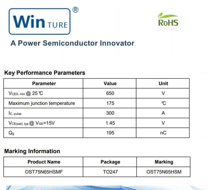
Key Performance Parameters
| Parameter | Value | Unit |
| VCES, min @ 25°C | 650 | V |
| Maximum junction temperature | 175 | °C |
| IC, pulse | 300 | A |
| VCE(sat), typ @ VGE=15V | 1.45 | V |
| Qg | 195 | nC |
| Product Name | Package | Marking |
| OST75N65HSMF | TO247 | OST75N65HSM |
| Parameter | Symbol | Value | Unit |
| Collector emitter voltage | VCES | 650 | V |
| Gate emitter voltage | VGES | ±20 | V |
| Transient gate emitter voltage, TP≤10µs, D<0.01 | ±30 | V | |
| Continuous collector current1) , TC=25ºC | IC | 90 | A |
| Continuous collector current1) , TC=100ºC | 75 | A | |
| Pulsed collector current2) , TC=25ºC | IC, pulse | 300 | A |
| Diode forward current1) , TC=25ºC | IF | 90 | A |
| Diode forward current1) , TC=100ºC | 75 | A | |
| Diode pulsed current2) , TC=25ºC | IF, pulse | 300 | A |
| Power dissipation3) , TC=25ºC | PD | 395 | W |
| Power dissipation3) , TC=100ºC | 198 | W | |
| Operation and storage temperature | Tstg, Tvj | -55 to 175 | °C |
| Parameter | Symbol | Value | Unit |
| IGBT thermal resistance, junction-case | RθJC | 0.38 | °C/W |
| Diode thermal resistance, junction-case | RθJC | 0.38 | °C/W |
| Thermal resistance, junction-ambient4) | RθJA | 40 | °C/W |
| Parameter | Symbol | Min. | Typ. | Max. | Unit | Test condition |
| Collector-emitter breakdown voltage | V(BR)CES | 650 | V | VGE=0 V, IC=0.5 mA | ||
Collector-emitter saturation voltage | VCE(sat) | 1.45 | 1.7 | V | VGE=15 V, IC=75 A Tvj=25°C | |
| 1.65 | V | VGE=15 V, IC=75 A, Tvj =125°C | ||||
| 1.75 | VGE=15 V, IC=75 A, Tvj =175°C | |||||
| Gate-emitter threshold voltage | VGE(th) | 3.0 | 4.0 | 5.0 | V | VCE=VGE , ID=0.5 mA |
Diode forward voltage | VF | 1.6 | 1.8 | V | VGE=0 V, IF=75 A Tvj =25°C | |
| 1.5 | VGE=0 V, IF=75 A, Tvj =125°C | |||||
| 1.4 | VGE=0 V, IF=75 A, Tvj =175°C | |||||
| Gate-emitter leakage current | IGES | 100 | nA | VCE=0 V, VGE=20 V | ||
| Zero gate voltage collector current | ICES | 10 | μA | VCE=650 V, VGE=0 V |
| Parameter | Symbol | Min. | Typ. | Max. | Unit | Test condition |
| Input capacitance | Cies | 8066 | pF | VGE=0 V, VCE=25 V, ƒ=100 kHz | ||
| Output capacitance | Coes | 230 | pF | |||
| Reverse transfer capacitance | Cres | 6 | pF | |||
| Turn-on delay time | td(on) | 68 | ns | VGE=15 V, VCC=400 V, RG=10 Ω, IC=75 A | ||
| Rise time | tr | 107 | ns | |||
| Turn-off delay time | td(off) | 265 | ns | |||
| Fall time | tf | 91 | ns | |||
| Turn-on energy | Eon | 2.98 | mJ | |||
| Turn-off energy | Eoff | 1.1 | mJ | |||
| Turn-on delay time | td(on) | 56 | ns | VGE=15 V, VCC=400 V, RG=10 Ω, IC=30 A | ||
| Rise time | tr | 49 | ns | |||
| Turn-off delay time | td(off) | 311 | ns | |||
| Fall time | tf | 62 | ns | |||
| Turn-on energy | Eon | 0.95 | mJ | |||
| Turn-off energy | Eoff | 0.34 | mJ |
| Parameter | Symbol | Min. | Typ. | Max. | Unit | Test condition |
| Total gate charge | Qg | 195 | nC | VGE=15 V, VCC=520 V, IC=75 A | ||
| Gate-emitter charge | Qge | 62 | nC | |||
| Gate-collector charge | Qgc | 54 | nC |
| Parameter | Symbol | Min. | Typ. | Max. | Unit | Test condition |
| Diode reverse recovery time | trr | 132 | ns | VR =400 V, IF=75 A, diF/dt=500 A/μs Tvj = 25°C | ||
| Diode reverse recovery charge | Qrr | 1.4 | μC | |||
| Diode peak reverse recovery current | Irrm | 20 | A |