 Complaint

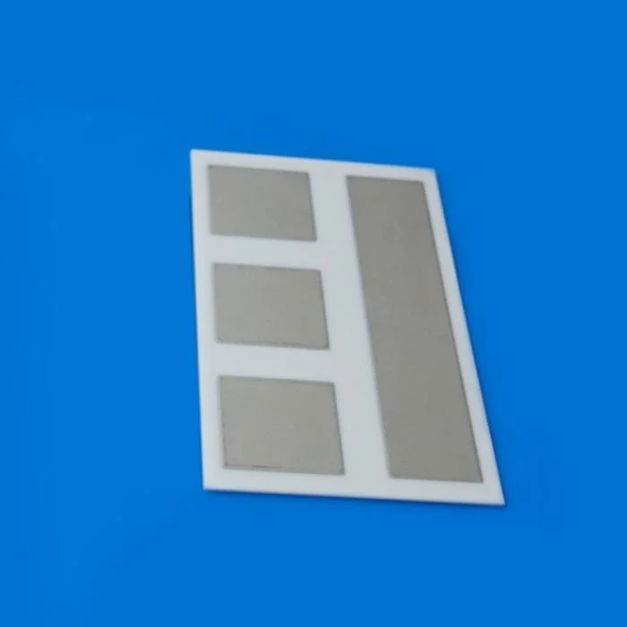
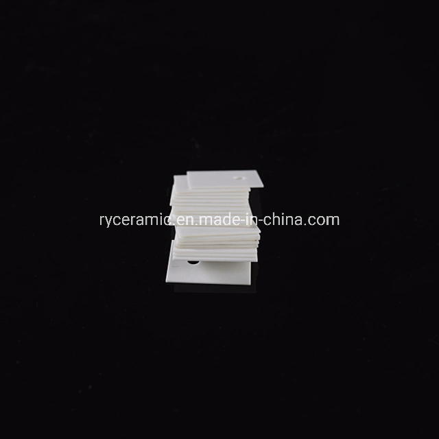
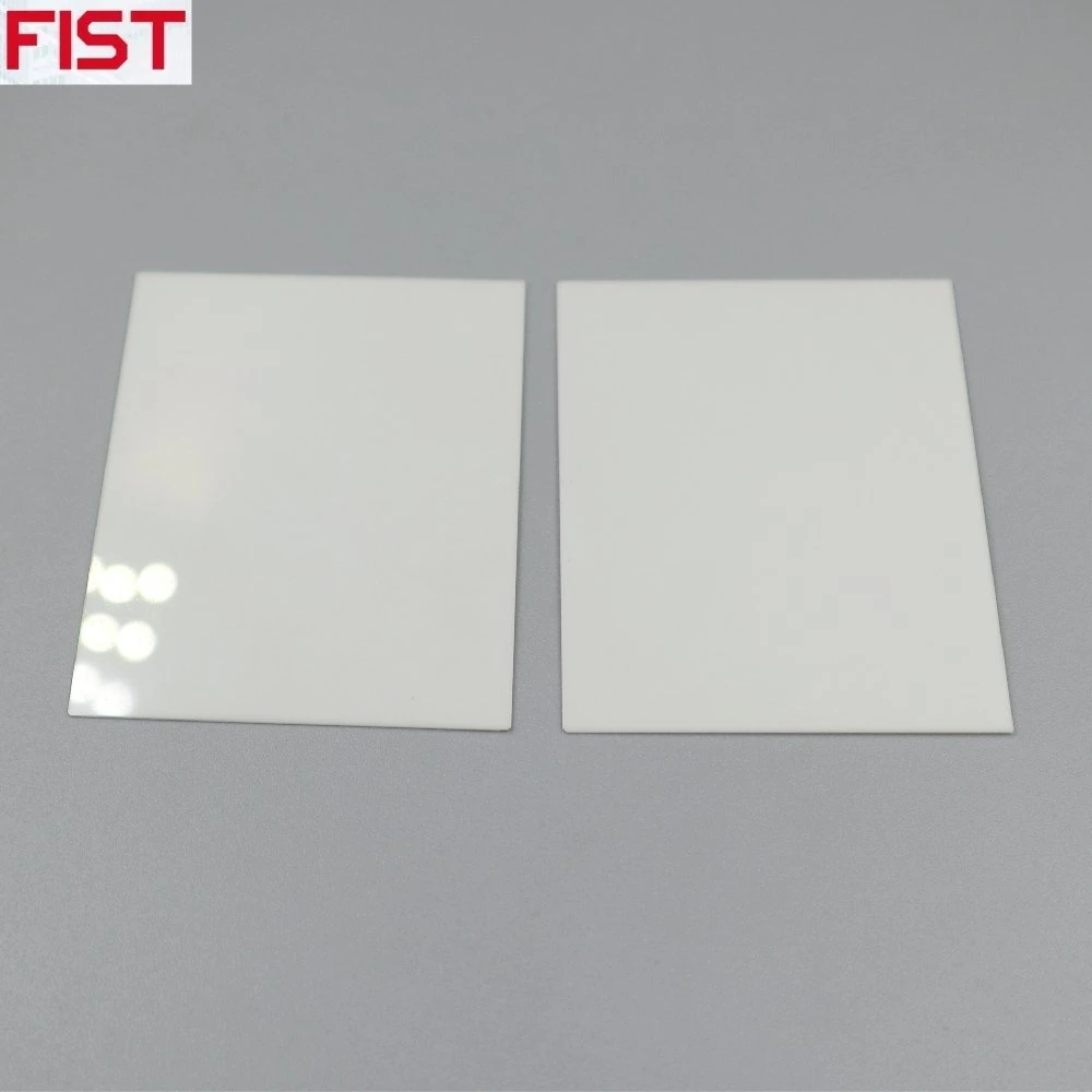
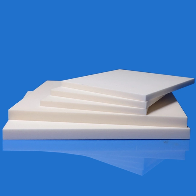
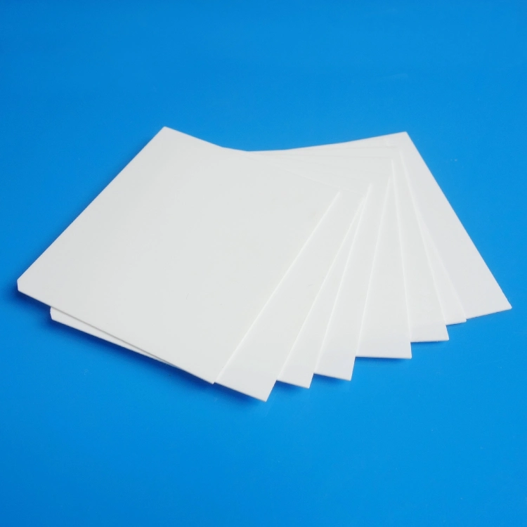
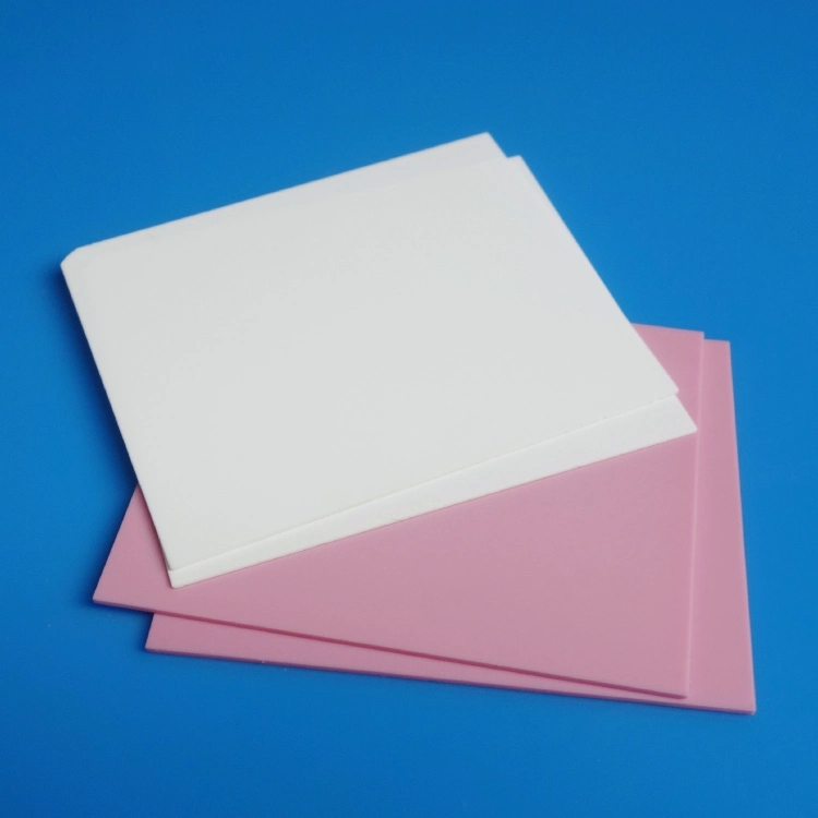
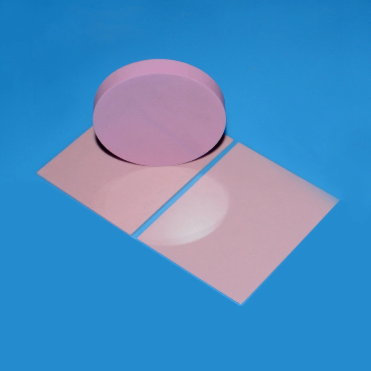
White 96% 99.6% Aluminum Oxide Al2O3 Alumina Ceramic Substrate for Circuit
Ceramic substrate is a commonly used electronic packaging substrate material. Compared with plastic and metal substrates, ceramic substrate has the following advantages:
1) Good Insulation
Generally speaking, the higher substrate resistance, the better reliability of the package. Ceramic materials are generally covalent bond compounds with better insulation properties.
2) Low Dielectric Coefficient and Good Frequency Performance
The low dielectric constant and dielectric loss of ceramic materials can reduce the signal delay time and increase the transmission speed.
3) Small Coefficient of Thermal Expansion (CTE)
Covalent bond compounds generally have high melting point, and the higher the melting point, the smaller the thermal expansion coefficient, so the CTE of ceramic materials is generally small.
4) High Thermal Conductivity
Ceramic substrate materials are widely used in high-reliability, high-frequency, high-temperature resistance, and strong air-tight product packaging in aviation, aerospace and military engineering. The packaging of ceramic substrate materials is generally a multilayer ceramic substrate package, which is widely used in hybrid integrated circuit (HIC) and multi-chip module (MCM) ceramic packages.
For material properties, please refer to the table below.
| Alumina Ceramic Substrate | ||||
| Item | Unit | 96% Al2O3 | 99.6% Al2O3 | |
| Mechanical Properties | ||||
| Color | / | / | White | Ivory |
| Density | Drainage Method | g/cm3 | ≥3.70 | ≥3.95 |
| Light Reflectivity | 400nm/1mm | % | 94 | 83 |
| Flexural Strength | Three Point Bending | MPa | >350 | >500 |
| Fracture Toughness | Indentation Method | MPa·m1/2 | 3.0 | 3.0 |
| Vickers Hardness | Load 4.9N | GPa | 14 | 16 |
| Young's Modulus | Stretching Method | GPa | 340 | 300 |
| Water Absorption | % | 0 | 0 | |
| Camber | / | Length‰ | T≤0.3: ≤5‰, Others: ≤3‰ | ≤3‰ |
| Thermal Properties | ||||
| Max. Service Temperature (Non-loading) | / | ºC | 1200 | 1400 |
| CTE (Coefficient of Thermal Expansion) | 20-800ºC | 1×10⁻⁶/ºC | 7.8 | 7.9 |
| Thermal Conductivity | 25ºC | W/m·K | >24 | >29 |
| Thermal Shock Resistance | 800ºC | ≥10 Times | No Crack | No Crack |
| Specific Heat | 25ºC | J/kg·k | 750 | 780 |
| Electrical Properties | ||||
| Dielectric Constant | 25ºC, 1MHz | / | 9.4 | 9.8 |
| Dielectric Loss Angle | 25ºC, 1MHz | ×10-4 | ≤3 | ≤2 |
| Volume Resistivity | 25ºC | Ω·cm | ≥1014 | ≥1014 |
| Dielectric Strength | DC | KV/mm | ≥15 | ≥15 |
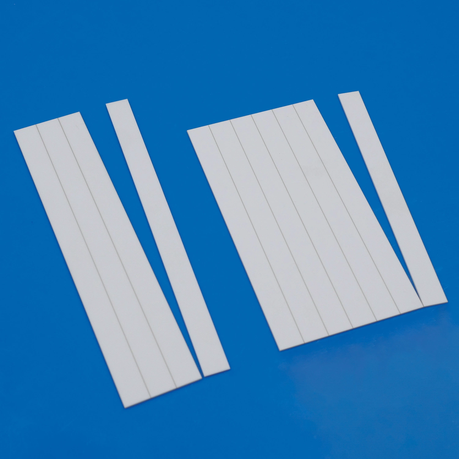
1. Product Specification
Products of various specifications can be produced. The table below shows our standard thicknesses and sizes.
| Alumina Ceramic Substrate | |||||||
| 99.6% Al2O3 | |||||||
| Thickness (mm) | Maximum Size (mm) | Shape | Molding Technique | ||||
| As Fired | Lapped | Polished | Rectangular | Square | Round | ||
| 0.1-0.2 | 50.8 | 50.8 | √ | √ | Tape Casting | ||
| 0.25 | 114.3 | 114.3 | √ | Tape Casting | |||
| 0.38 | 120 | 114.3 | 114.3 | √ | Tape Casting | ||
| 0.5 | 120 | 114.3 | 114.3 | √ | Tape Casting | ||
| 0.635 | 120 | 114.3 | 114.3 | √ | Tape Casting | ||
| Other special thicknesses within the thickness range of 0.1-0.635mm can be achieved by lapping. | |||||||
| 96% Al2O3 | |||||||
| Thickness (mm) | Maximum Size (mm) | Shape | Molding Technique | ||||
| As Fired | Lapped | Polished | Rectangular | Square | Round | ||
| 0.25 | 120 | 114.3 | 114.3 | √ | Tape Casting | ||
| 0.3 | 120 | 114.3 | 114.3 | √ | Tape Casting | ||
| 0.38 | 140×190 | √ | Tape Casting | ||||
| 0.5 | 140×190 | √ | Tape Casting | ||||
| 0.635 | 140×190 | √ | Tape Casting | ||||
| 0.76 | 130×140 | √ | Tape Casting | ||||
| 0.8 | 130×140 | √ | Tape Casting | ||||
| 0.89 | 130×140 | √ | Tape Casting | ||||
| 1 | 280×240 | √ | Tape Casting | ||||
| 1.5 | 165×210 | √ | Tape Casting | ||||
| 2 | 500×500 | √ | Tape Casting | ||||
| Other special thicknesses within the thickness range of 0.1-2.0mm can be achieved by lapping. | |||||||
| Alumina Ceramic Substrate | ||||
| Item | Substrate Thickness (mm) | Standard Tolerance (mm) | Best Tolerance (mm) | Laser Cutting Tolerance (mm) |
| Length and Width Tolerance | / | ±2 | ±0.15 | |
| Thickness Tolerance | T<0.3 | ±0.03 | ±0.01 | |
| 0.30-1.0 | ±0.05 | ±0.01 | ||
| T>1.0 | ±10% | ±0.01 | ||
| Alumina Ceramic Substrate | |||
| Material | Surface Roughness (μm) | ||
| As Fired | Lapped | Polished | |
| 96% Al2O3 | Ra 0.2-0.75 | Ra 0.3-0.7 | Ra ≤0.05 |
| 99.6% Al2O3 | Ra 0.05-0.15 | Ra 0.1-0.5 | Ra ≤0.05 |
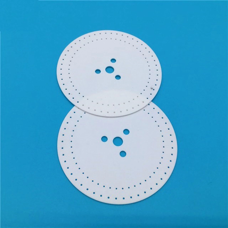
| Alumina Ceramic Substrate | |
| Hole Diameter (mm) | Standard Tolerance (mm) |
| φ≤0.5 | 0.08 |
| φ>0.5 | 0.2 |
| Alumina Ceramic Substrate | |
| Substrate Thickness (mm) | the Percentage of Laser Scribe Line Depth to Thickness (%) |
| 0.2-0.3 | 40%±5% |
| 0.3<T≤0.5 | 50%±3% |
| 0.5<T≤1.0 | 43%±3% |
| 1.2 | 55%±3% |
| 1.5 | 55%±3% |
| 2.0 | 55%+10% |
| The scribing spot can be in different sizes. Generally there are small spot 0.03-0.04mm (Substrate Thickness≤0.5mm ) and large spot 0.08-0.1mm (Substrate Thickness>0.5mm), and the accuracy is ±0.01mm. | |
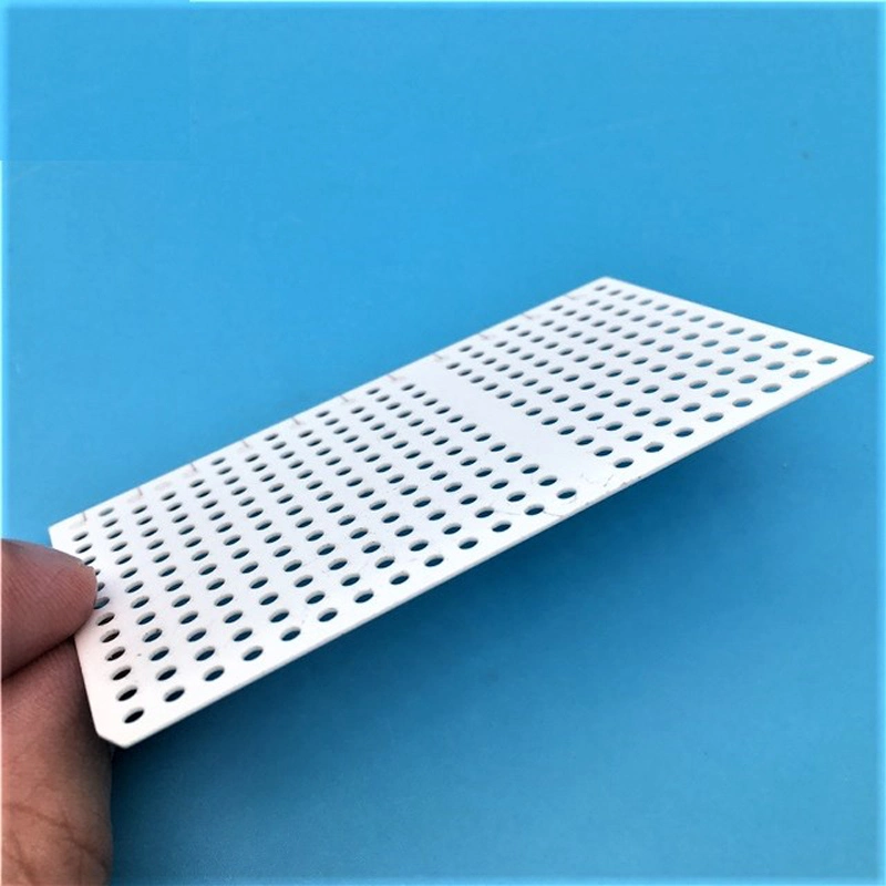
The company has a strong processing capacity. We offer bare ceramic substrates in various raw materials, sizes, shapes and thicknesses.