 Complaint

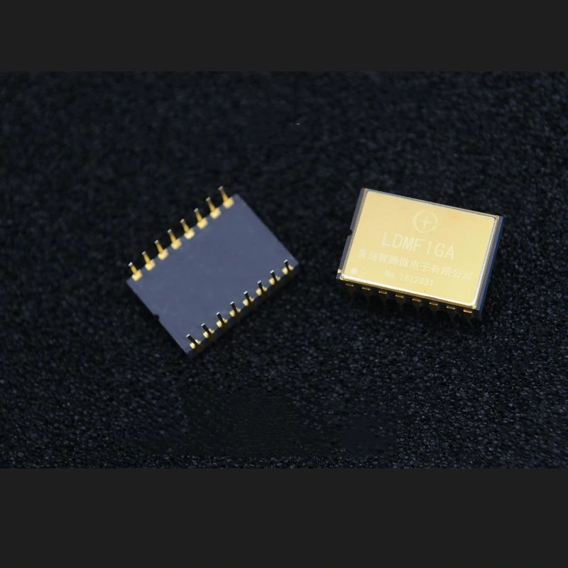
Pin Description:
| PIN | Functional description |
| IO0 ~ IO7 | Multiplexed input / output The bidirectional I/Os transfer address, data, and command information. When C(-)E(-) pin is high,the I/Os is High impedance. |
| CLE | Command Latch Enable When CLE is high, the command is latched into the command register through the IO port on the rising edge of the signal. |
| ALE | Address Latch Enable When ALE is high,the address is latched into the address register through the IO port on the rising edge of the signal. |
| C(-)E(-) | Chip Enable Enables or disables the chip. |
| R(-)E(-) | Read Enable Control the output of serial data. When the signal is low, the data is driven to the IO port. Data is valid after tREA time on the falling edge of R(-)E(-), and the internal column address counter is incremented automatically. |
| W(-)E(-) | Write Enable Control the input of serial data,command, address and data is latched on the W(-)E(-) Rising edge. |
| R/B(-) | Ready/Busy output Indicates the device operating state. When low, indicates that programming, erase, or random read operation is in progress, when high, indicates that no operation or operation is finished. It is recommended to connect a pull-up resistor (4.7K~10K) to the pin. |
| Vcc | Power Supply |
| Vss | GND |
| Addressing | IO 0 | IO 1 | IO 2 | IO 3 | IO 4 | IO 5 | IO 6 | IO 7 | |
| 1st cycle | CA0 | CA1 | CA2 | CA3 | CA4 | CA5 | CA6 | CA7 | Column Address 1 |
| 2nd cycle | CA8 | CA9 | CA10 | CA11 | 0 | 0 | 0 | 0 | Column address 2 |
| 3rd cycle | PA0 | PA1 | PA2 | PA3 | PA4 | PA5 | PA6 | BA7 | Row address 1 |
| 4th cycle | BA8 | BA9 | BA10 | BA11 | BA12 | BA13 | BA14 | BA15 | Row address 2 |
| 5th cycle | BA16 | BA17 | BA18 | 0 | 0 | 0 | 0 | 0 | Row address 3 |
| Addressing | IO 0 | IO 1 | IO 2 | IO 3 | IO 4 | IO 5 | IO 6 | IO 7 | |
| 1st cycle | CA0 | CA1 | CA2 | CA3 | CA4 | CA5 | CA6 | CA7 | Column Address 1 |
| 2nd cycle | CA8 | CA9 | CA10 | CA11 | CA12 | CA13 | 0 | 0 | Column address 2 |
| 3rd cycle | PA0 | PA1 | PA2 | PA3 | PA4 | PA5 | PA6 | BA7 | Row address 1 |
| 4th cycle | BA8 | BA9 | BA10 | BA11 | BA12 | BA13 | BA14 | BA15 | Row address 2 |
| 5th cycle | BA16 | BA17 | BA18 | 0 | 0 | 0 | 0 | 0 | Row address 3 |
| Function | 1st cycle | 2nd cycle |
| Reset | FFh | - |
| Read | 00h | 30h |
| Page program | 80h | 10h |
| Block erase | 60h | D0h |
| Symbol | MIN | Standard | MAX | Units | Dscription |
| tPROG | 0.8 | 3 | ms | Page program time | |
| tBERS | 1.5 | 10 | ms | Block erasure time | |
| tCLS | 15 | ns | |||
| tCLH | 5 | ns | |||
| tCS | 20 | ns | |||
| tCH | 5 | ns | |||
| tWP | 15 | ns | |||
| tALS | 15 | ns | |||
| tALH | 5 | ns | |||
| tDS | 15 | ns | |||
| tDH | 5 | ns | |||
| tWC | 30 | ns | |||
| tWH | 10 | ns | |||
| tADL | 70 | ns | |||
| tR | 60 | μs | |||
| tAR | 10 | ns | |||
| tCLR | 10 | ns | |||
| tRR | 20 | ns | |||
| tRP | 15 | ns | |||
| tWB | 100 | ns | |||
| tRC | 30 | ns | |||
| tREA | 20 | ns | |||
| tCEA | 25 | ns | |||
| tRHZ | 100 | ns | |||
| tCHZ | 30 | ns | |||
| tCSD | 10 | ns | |||
| tRHOH | 15 | ns | |||
| tRLOH | 5 | ns | |||
| tCOH | 15 | ns | |||
| tREH | 10 | ns | |||
| tIR | 0 | ns | |||
| tRHW | 100 | ns | |||
| tWHR | 60 | ns | |||
| tRST | 5/10/500 | μs | Read/programming/erasing |
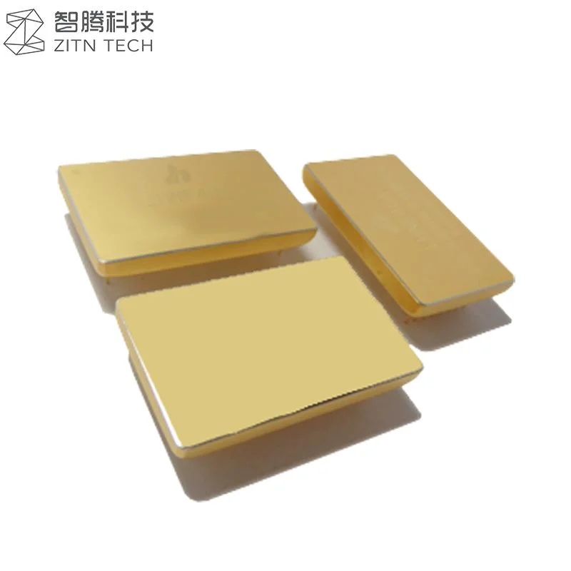
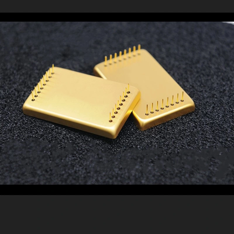
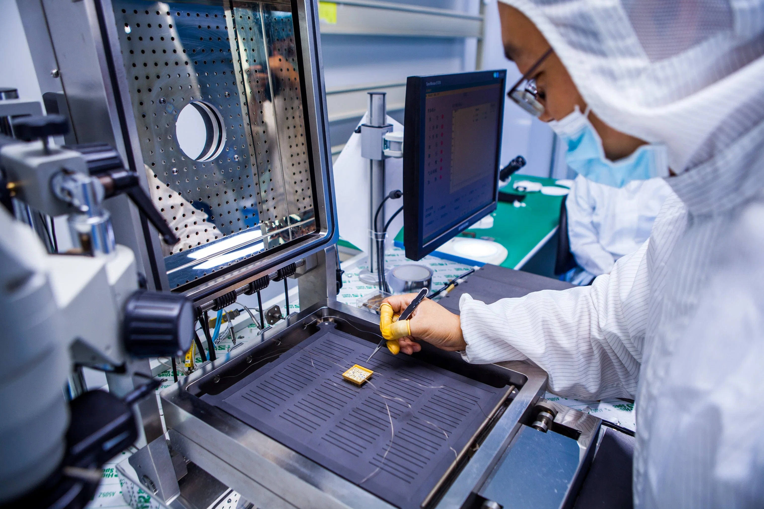
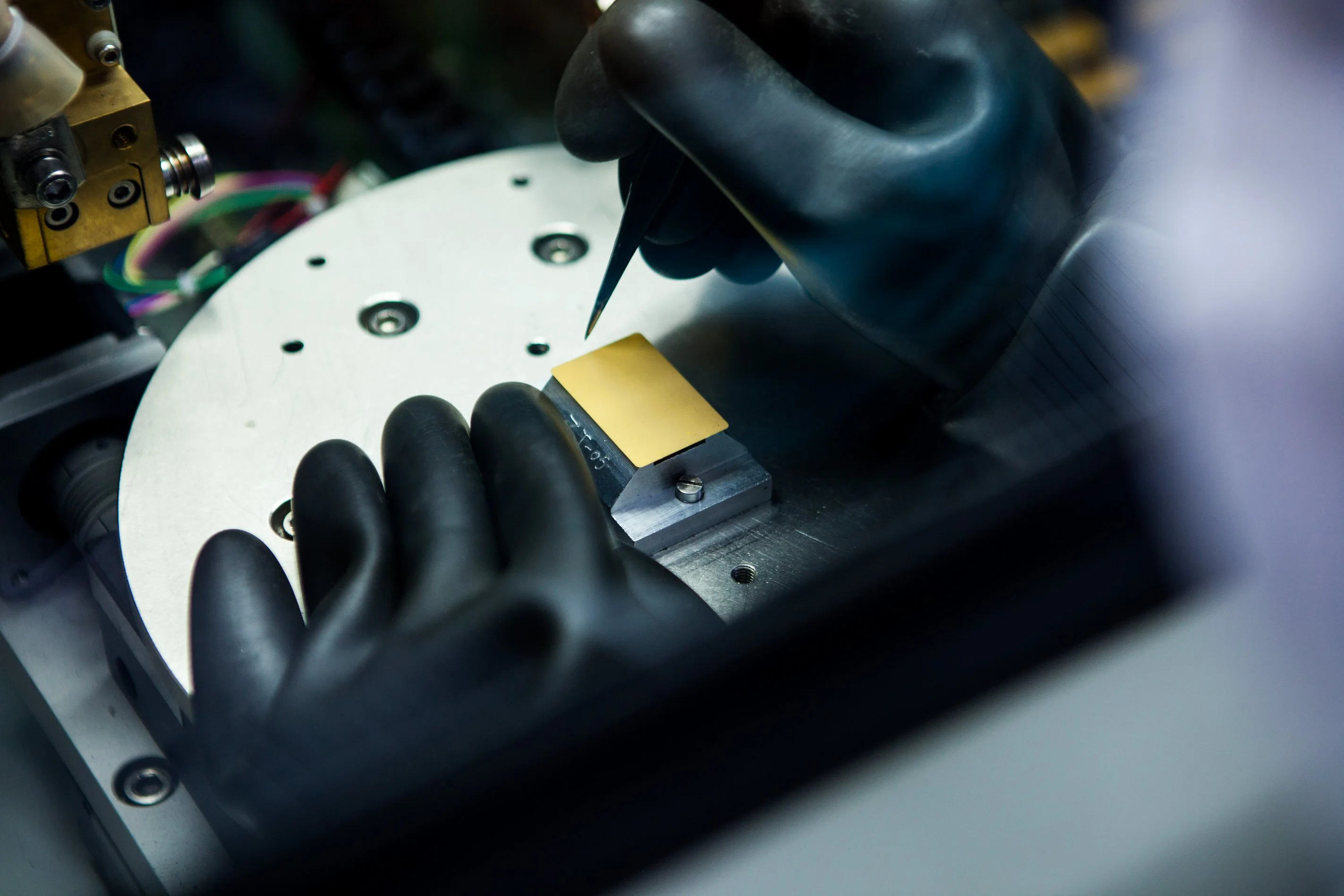
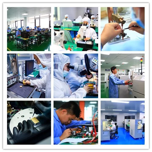
ZITN is a national high-tech enterprise, it was established in 2002 by many high tech engineers who have vast experience in microelectronic Industry. With 19 years' development, ZITN became a recognized industry leader in China, and we have total 175 employees, more than 49% of them are from R&D team. We mainly design, develop and manufacture high accuracy inclinometer, quartz based accelerometers, inertial measurement unit systems, IF Circuit products and Nand flash memory which widely used for aerospace, oil and gas drilling, geological exploration fields.
a. Experience in the hybrid thick film IC &high end sensors development and manufacture fields more than 19 years.
b. Invention patents more than 40 projects.
c. Scientific institution, production base more than 20000 square meters.
d. More than 49% of employees are from R&D team.
e. New cooperating customers more than1000 in recently 3 years.
f. Production capacity more than 100000/year;
g. Professional pre-sales, after-sales guide, solutions can be provided based on customers inquiries.
h. Customized Service.
Miniature volume ! Independent creative technology!
From the servo-circuit production to assmble the sensors at one-stop .
Customized anti-static box.
Delivery via express (DHL, Fedex, TNT, UPS etc...)
Delivery date within 7-10 days after the shipment from our factory.
What kind of service can you provide?
Except the stanadrd model, we also can provide the products accorded with customers' detailed requirments, such as calibration, repair, upgrade etc...
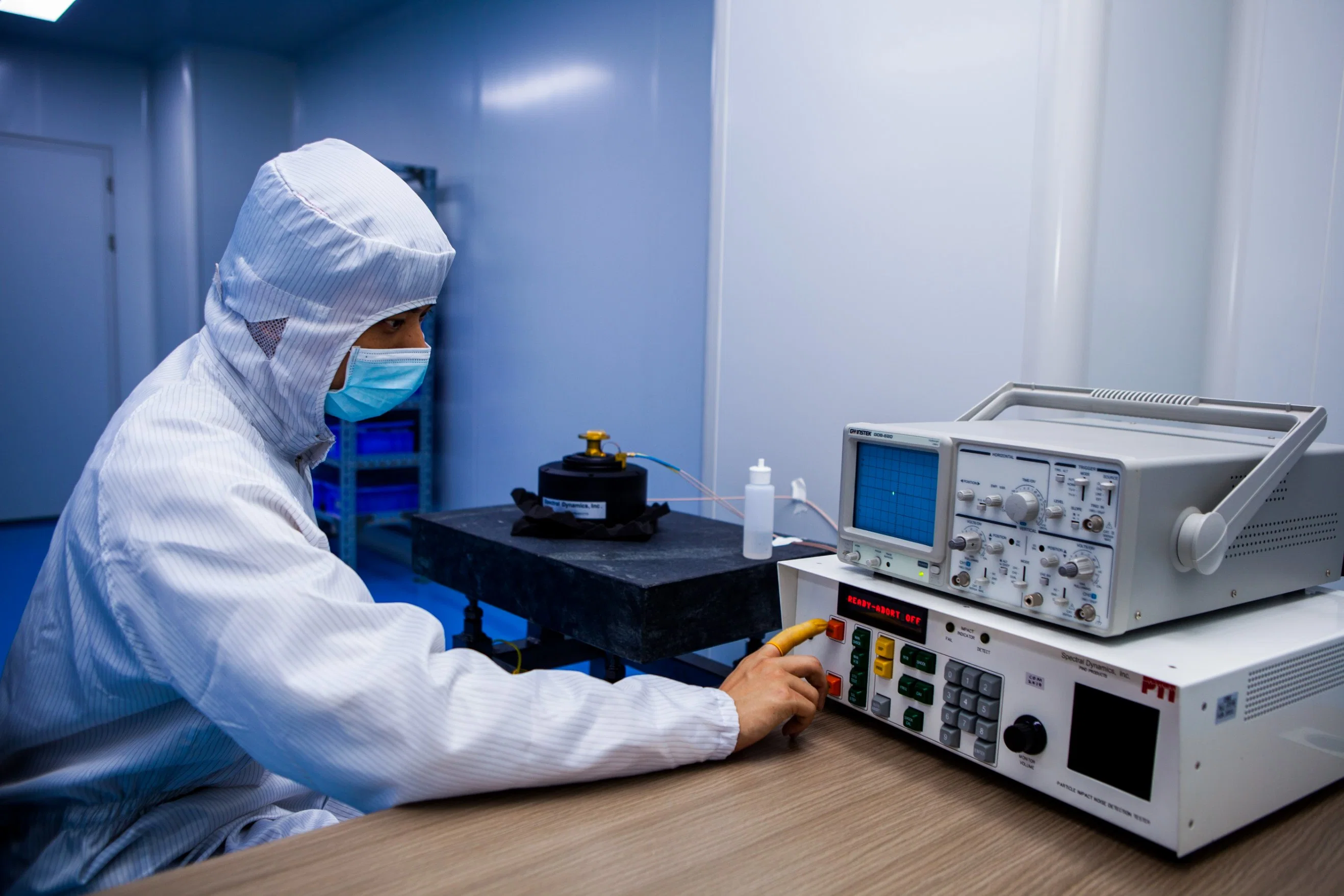
What kind of test of the product will be done before leave your factory?
We have a strict quality control system to guarantee the product performance, such as Non-magnetic turntable calibration system, Shock&Vibration test system, temperature cycle test system etc...
Can I get a sample for evaluation?
Yes, we're willing to provide the sample for evaluation and guide you for any techical questions in the whole process.