
 Complaint

| AlN Ceramic Substrate | ||
| Item | Unit | Value |
| Mechanical Properties | ||
| Color | / | Gray |
| Density | g/cm³ | ≥3.33 |
| Flexural Strength | MPa | ≥380 |
| Water Absorption | % | 0 |
| Camber | Length‰ | ≤3‰ |
| Thermal Properties | ||
| Max. Service Temperature (Non-loading) | ºC | >1000 |
| CTE (Coefficient of Thermal Expansion) | 20-800ºC, 1×10⁻⁶/ºC | 4-6 |
| Thermal Conductivity | 20ºC, W/m·K | 170-230 |
| Electrical Properties | ||
| Dielectric Constant | 1MHz | 8-10 |
| Volume Resistivity | 20ºC, Ω·cm | ≥1013 |
| Dielectric Strength | KV/mm | ≥17 |
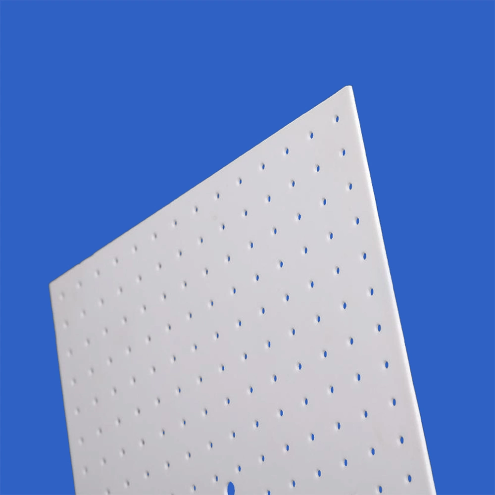
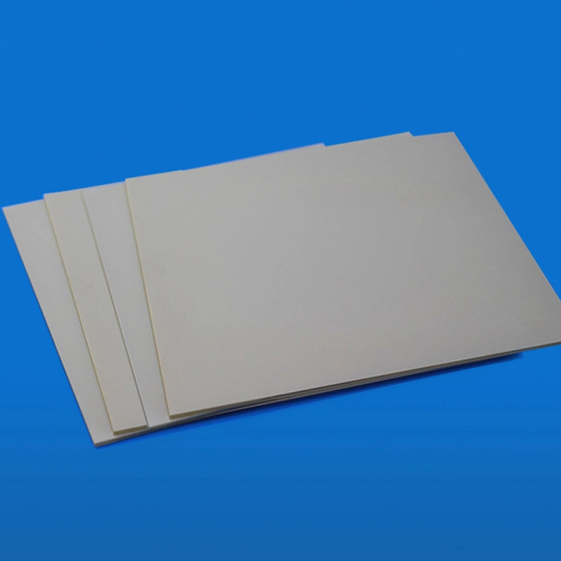
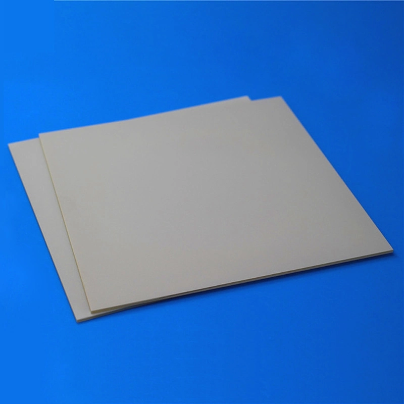
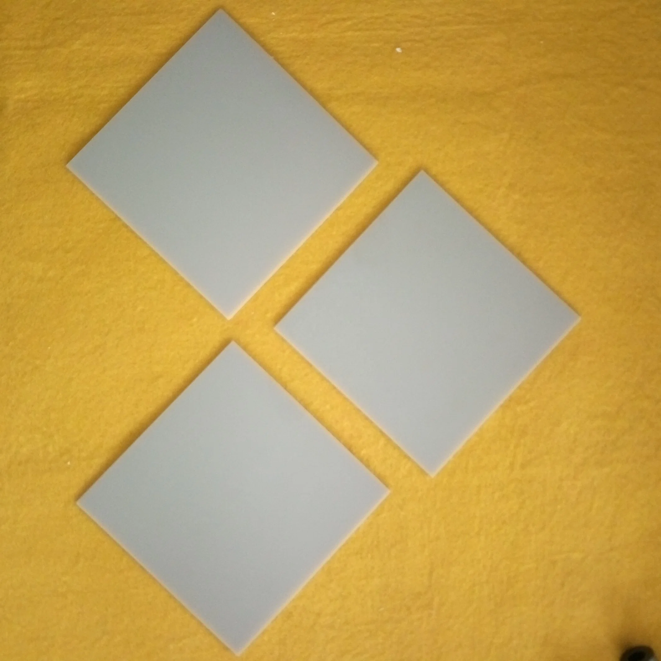
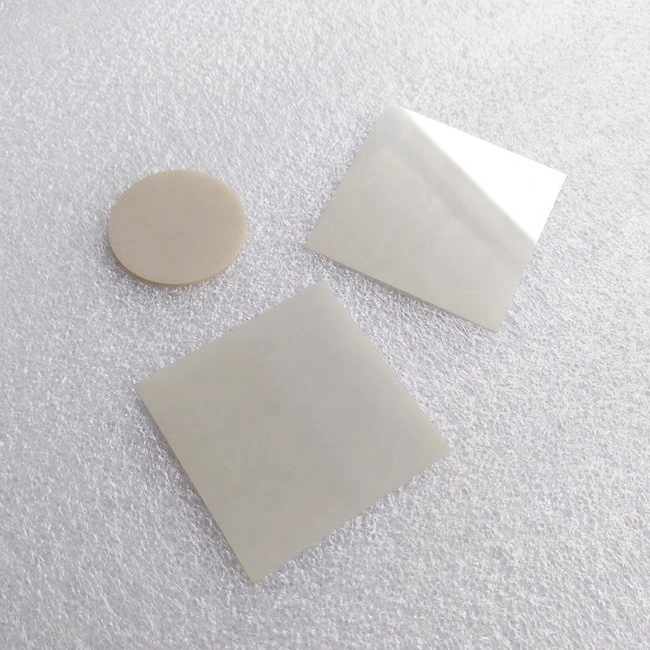
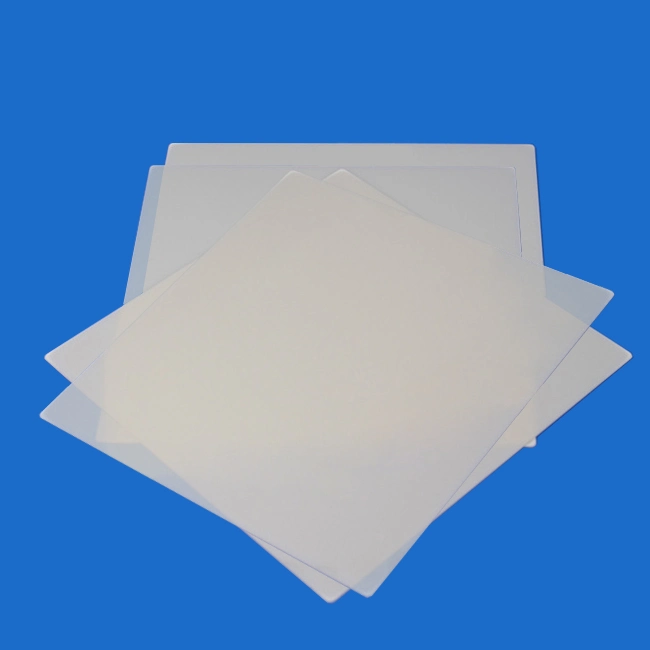
1. Product Specification
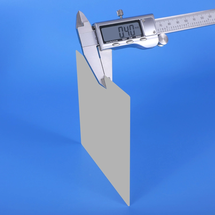
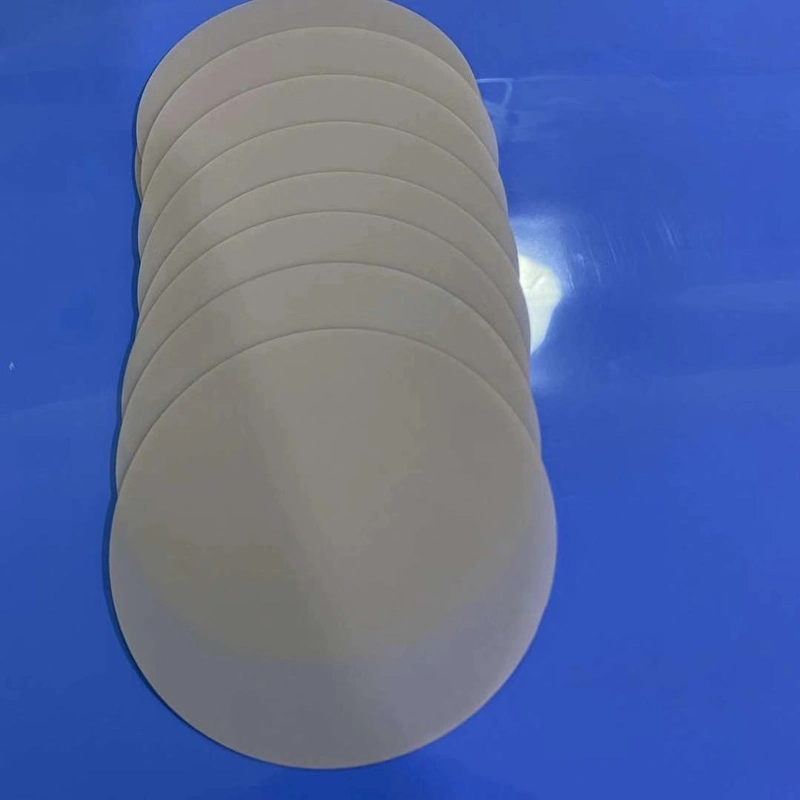
Products of various specifications can be produced. The table below shows our standard thicknesses and sizes.
| AlN Ceramic Substrate | |||||||
| Thickness (mm) | Maximum Size (mm) | Shape | Molding Technique | ||||
| As-fired | Lapped | Polished | Rectangular | Square | Round | ||
| 0.1-0.2 | 50.8 | 50.8 | √ | √ | Tape Casting | ||
| ≥0.2 | 114.3 | 114.3 | √ | √ | Tape Casting | ||
| 0.38 | 140×190 | 140×190 | 120 | √ | √ | Tape Casting | |
| 0.5 | 140×190 | 140×190 | 120 | √ | √ | Tape Casting | |
| 0.635 | 140×190 | 200 | 200 | √ | √ | √ | Tape Casting |
| 1 | 140×190 | 300 | 200 | √ | √ | √ | Tape Casting |
| 1.5 | 300 | 200 | √ | √ | Tape Casting | ||
| 2 | 300 | 200 | √ | √ | Tape Casting | ||
| 2.5 | 300 | √ | √ | Tape Casting | |||
| 3 | 300 | √ | √ | Tape Casting | |||
| … | 450 | √ | √ | Isostatic Pressing | |||
| 10 | 450 | √ | √ | Isostatic Pressing | |||
| Other special thicknesses within the thickness range of 0.1-3.0mm can be achieved by lapping. | |||||||
| AlN Ceramic Substrate | ||||
| Item | Substrate Thickness (mm) | Standard Tolerance (mm) | Best Tolerance (mm) | Laser Cutting Tolerance (mm) |
| Length and Width Tolerance | / | ±2 | ±0.15 | |
| Thickness Tolerance | T<1.0 | ±0.03 | ±0.01 | |
| 1.0≤T<1.5 | ±0.05 | ±0.01 | ||
| T≥1.5 | ±0.07 | ±0.01 | ||
| AlN Ceramic Substrate | |||
| Material | Surface Roughness (μm) | ||
| As Fired | Lapped | Polished | |
| AIN | Ra 0.4 | Ra 0.3-0.7 | Ra ≤0.05 |
| AlN Ceramic Substrate | |
| Hole Diameter (mm) | Standard Tolerance (mm) |
| φ≤0.5 | 0.08 |
| φ>0.5 | 0.2 |
| AlN Ceramic Substrate | |
| Substrate Thickness (mm) | the Percentage of Laser Scribe Line Depth to Thickness (%) |
| 0.2-0.3 | 40%±5% |
| 0.5<T≤1.0 | 50%±3% |
| 1.0<T≤1.2 | 55%±3% |
| 1.2<T≤1.5 | 60%±3% |
| 2.0 | 45% (Extreme Depth) |
| The scribing spot can be in different sizes. Generally there are small spot 0.03-0.04mm (Substrate Thickness≤0.5mm ) and large spot 0.08-0.1mm (Substrate Thickness>0.5mm), and the accuracy is ±0.01mm. | |
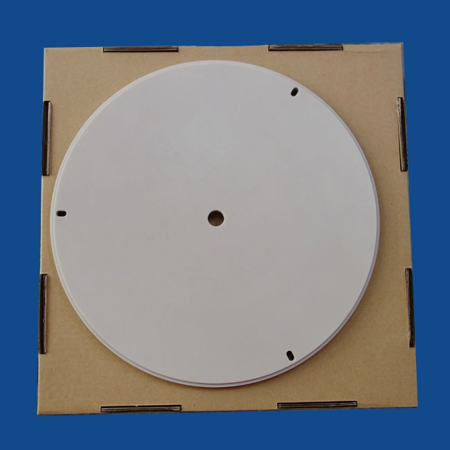
Because ceramics are hard and brittle materials, each of our products will be packed in a safe and reliable way to avoid damage during transportation.