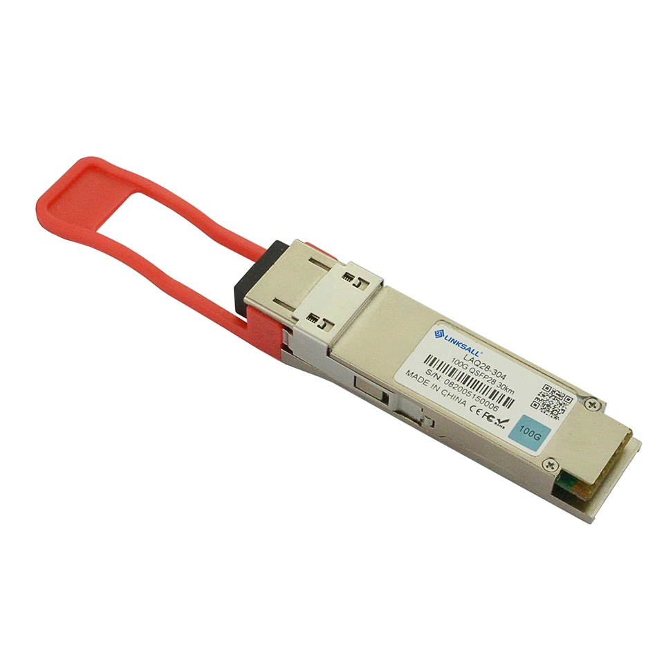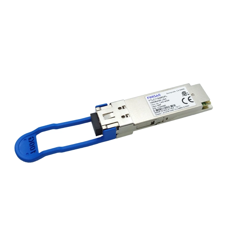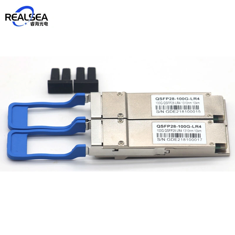
 Complaint

| Parameter | Test Point | Min | Typical | Max | Unit | Notes |
| Power Consumption | 3.5 | W | ||||
| Supply Current | Icc | 1.12 | A | |||
| Transceiver Power-onInitialization Time | 2000 | ms | 1 | |||
| Single-ended Input VoltageTolerance (Note 2) | -0.3 | 4.0 | V | Referred to TP1 signal common | ||
| AC Common Mode InputVoltage Tolerance | 15 | mV | RMS | |||
| Differential Input VoltageSwing Threshold | 50 | mVpp | LOSA Threshold | |||
| Differential Input VoltageSwing | Vin,pp | 190 | 700 | mVpp | ||
| Differential Input Impedance | Zin | 90 | 100 | 110 | Ohm | |
| Single-ended Output Voltage | -0.3 | 4.0 | V | Referred to signal common | ||
| AC Common Mode OutputVoltage | 7.5 | mV | RMS | |||
| Differential Output VoltageSwing | Vout,pp | 300 | 850 | mVpp | ||
| Differential Output Impedance | Zout | 90 | 100 | 110 | Ohm |
| Parameter | Symbol | Min | Typical | Max | Unit | Notes |
| Wavelength Assignment | L0 | 1294.53 | 1295.56 | 1296.59 | nm | |
| L1 | 1299.02 | 1300.05 | 1301.09 | nm | ||
| L2 | 1303.54 | 1304.58 | 1305.63 | nm | ||
| L3 | 1308.09 | 1309.14 | 1310.19 | nm | ||
| Transmitter | ||||||
| Side Mode Suppression Ratio | SMSR | 30 | dB | |||
| Total Average Launch Power | PT | 10.5 | dBm | |||
| Average Launch Power,each Lane | PAVG | -4.3 | 4.5 | dBm | ||
| OMA, each Lane | POMA | -1.3 | 4.5 | dBm | 1 | |
| Difference in Launch Power | Ptx,diff | 5 | dB | |||
| between any Two Lanes (OMA) | ||||||
| Launch Power in OMA minus Transmitter and Dispersion Penalty (TDP), each Lane | -2.3 | dBm | ||||
| TDP, each Lane | TDP | 2.2 | dB | |||
| Extinction Ratio | ER | 4 | dB | |||
| Relative Intensity Noise | RIN | -130 | dB/Hz | |||
| Optical Return Loss Tolerance | TOL | 20 | dB | |||
| Transmitter Reflectance | RT | -12 | dB | |||
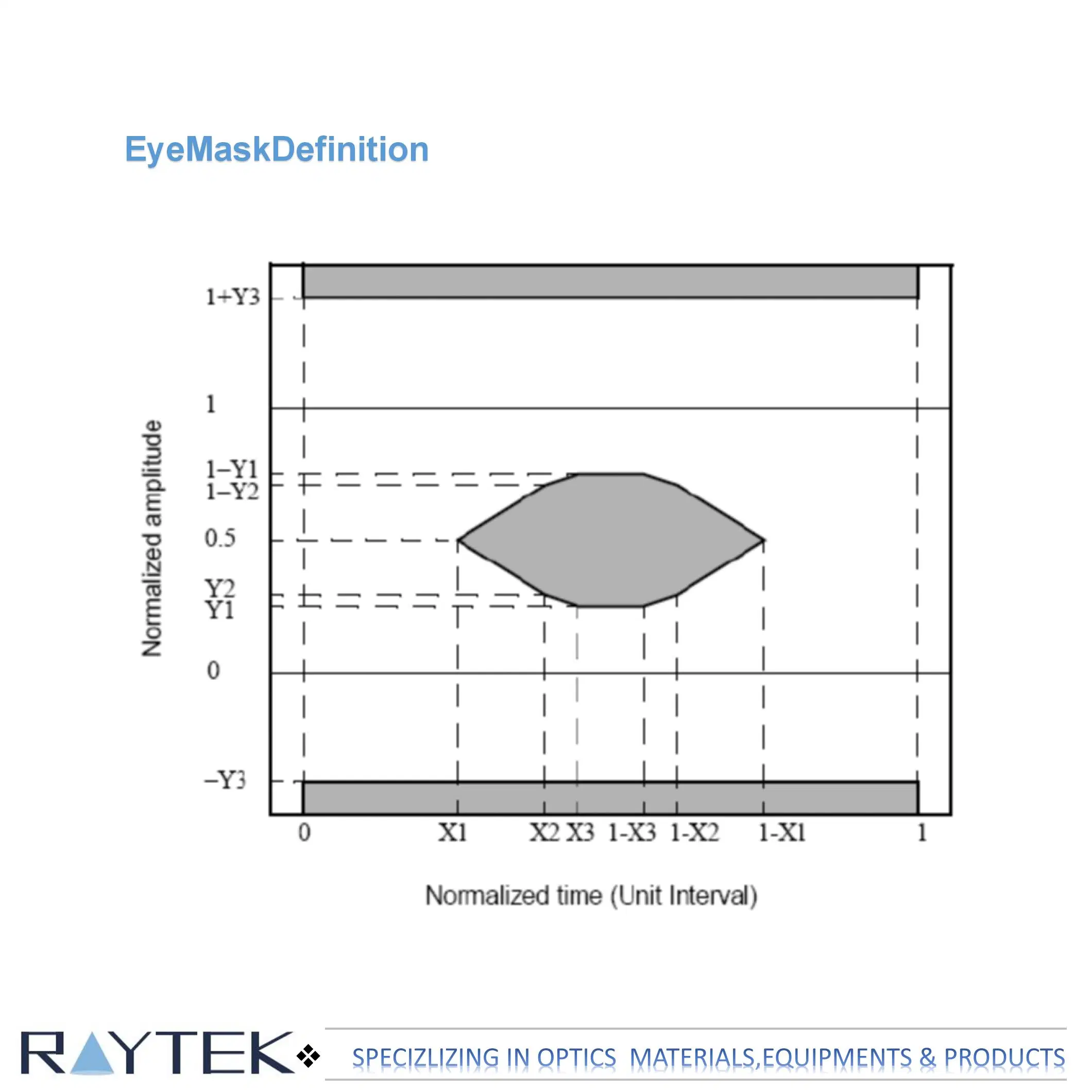
| Eye Mask{X1, X2, X3, Y1, Y2, Y3} | {0.25, 0.4, 0.45, 0.25, 0.28, 0.4} | 2 | ||||
| Average Launch Power OFF Transmitter, each Lane | Poff | -30 | dBm | |||
| Receiver | ||||||
| Damage Threshold, each Lane | THd | 5.5 | dBm | 3 | ||
| Total Average Receive Power | 10.5 | dBm | ||||
| Average Receive Power, each Lane | -10.6 | 4.5 | dBm | |||
| Receive Power (OMA), each Lane | 4.5 | dBm | ||||
| Receiver Sensitivity (OMA), eachLane | SEN | -10.6 | dBm | |||
| Stressed Receiver Sensitivity(OMA), each Lane | -6.8 | dBm | 4 | |||
| Receiver Reflectance | RR | -26 | dB | |||
| Difference in Receive Power between any Two Lanes (OMA) | Prx,diff | 5.5 | dB | |||
| LOS Assert | LOSA | -24 | -13.6 | dBm | ||
| LOS Deassert | LOSD | -11.6 | dBm | |||
| LOS Hysteresis | LOSH | 1.5 | dB | |||
| Receiver Electrical 3 dB upper Cutoff Frequency, each Lane | Fc | 31 | GHz | |||
| Conditions of Stress Receiver Sensitivity Test (Note 5) | ||||||
| Vertical Eye Closure Penalty, eachLane | 1.8 | dB | ||||
Stressed Eye J2 Jitter, each Lane | 0.3 | UI | ||||
| Stressed Eye J9 Jitter, each Lane | 0.47 | UI | ||||
| Parameter | Symbol | Min | Max | Unit | Notes |
| Temperature monitor absolute error | DMI_Temp | -3 | 3 | degC | Over operating temp |
| Supply voltage monitor absolute error | DMI _VCC | -0.1 | 0.1 | V | Full operating range |
| Channel RX power monitor absolute error | DMI_RX | -3 | 3 | dB | Per channel |
| Channel Bias current monitor | DMI_Ibias | -10% | 10% | mA | Per channel |
| Channel TX power monitor absolute error | DMI_TX | -3 | 3 | dB | Per channel |