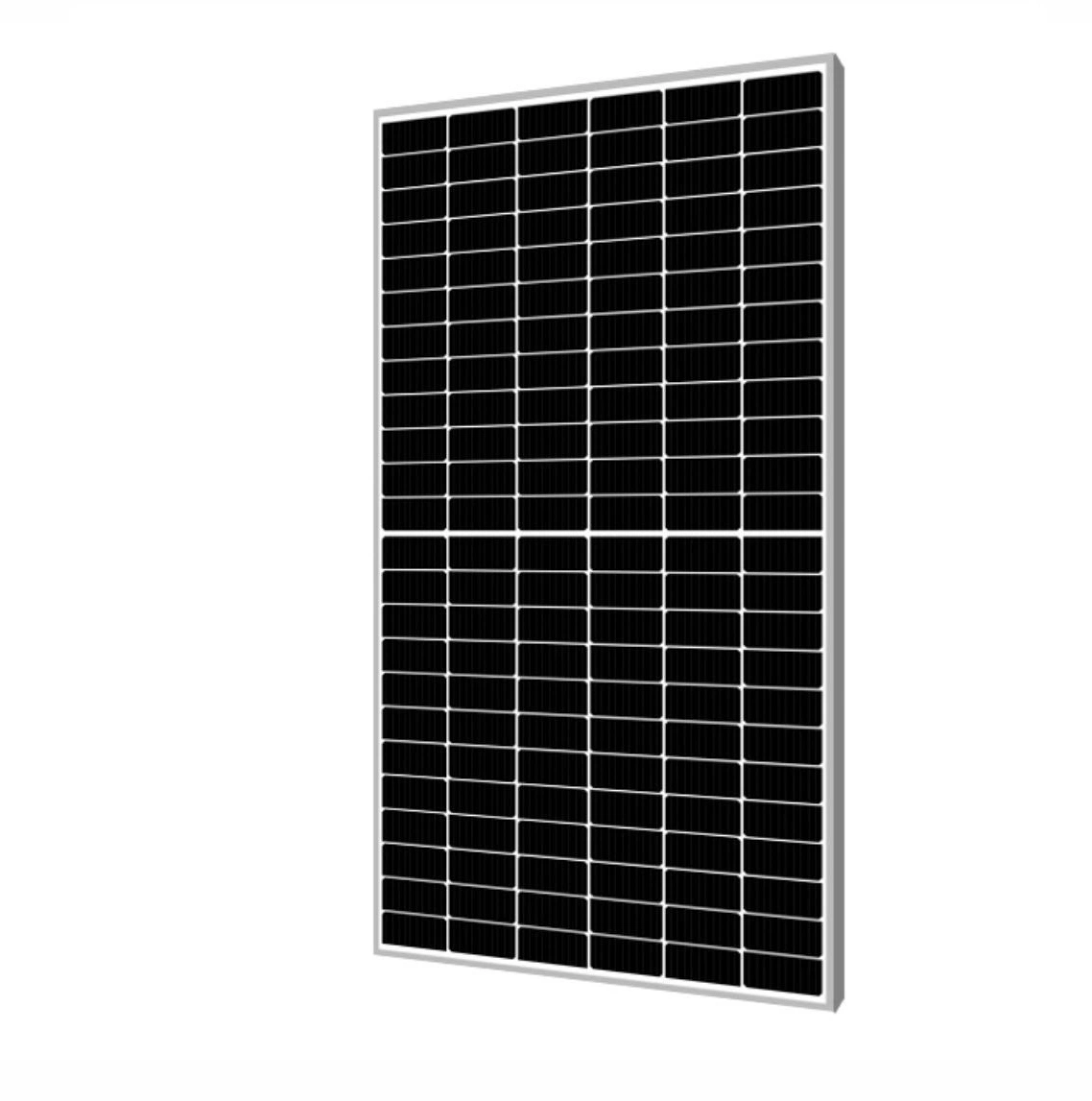
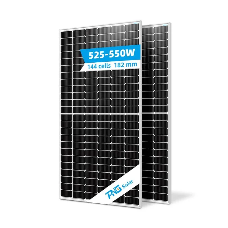
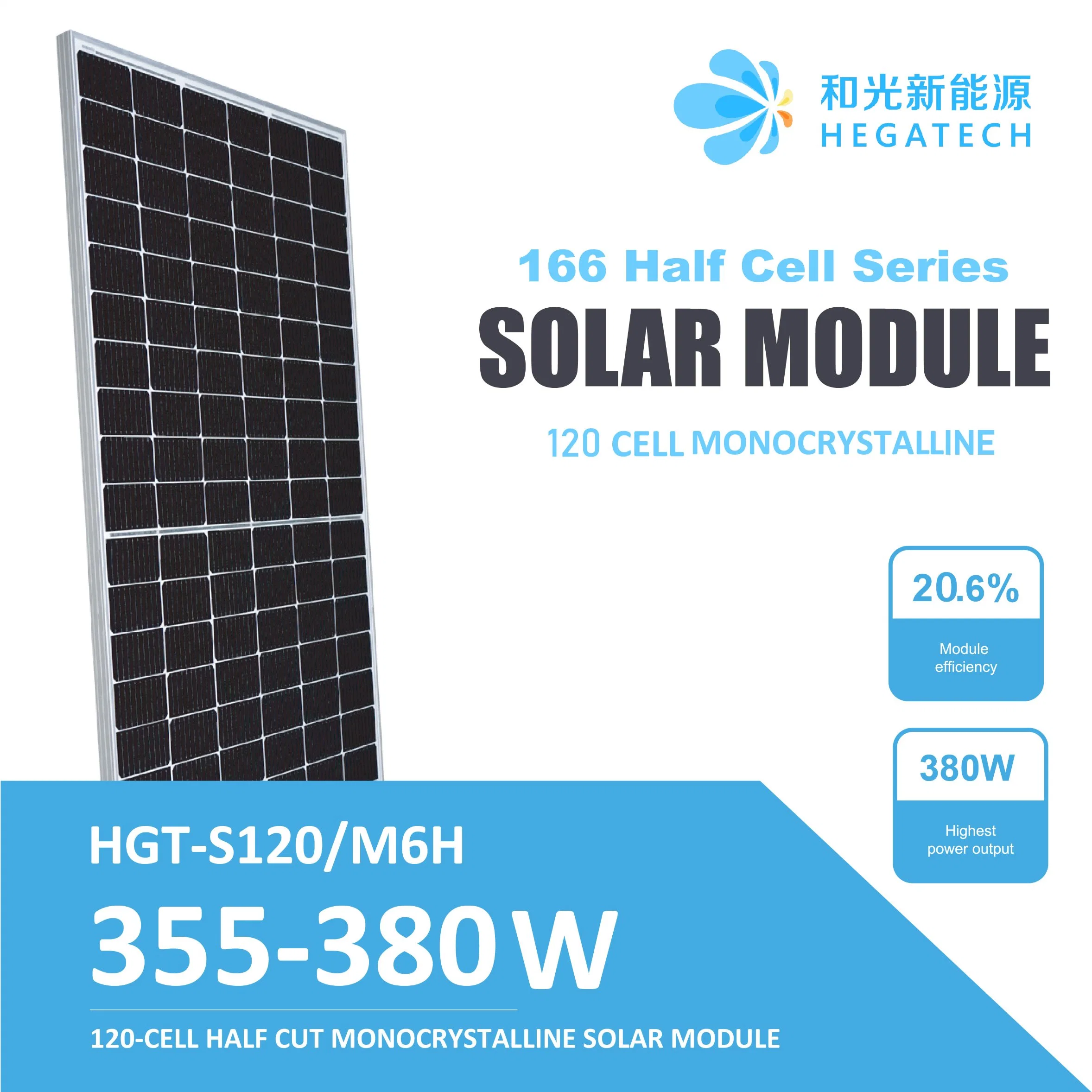
Description
Product Description
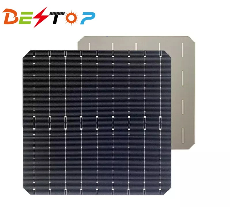
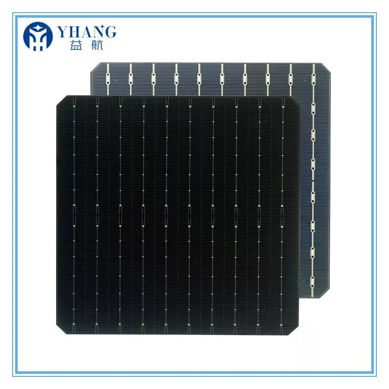
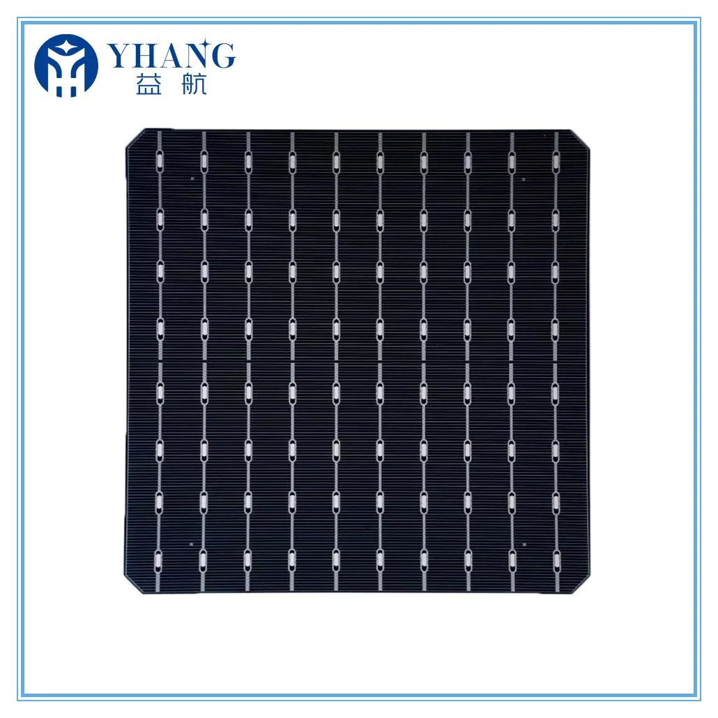
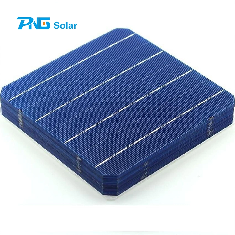
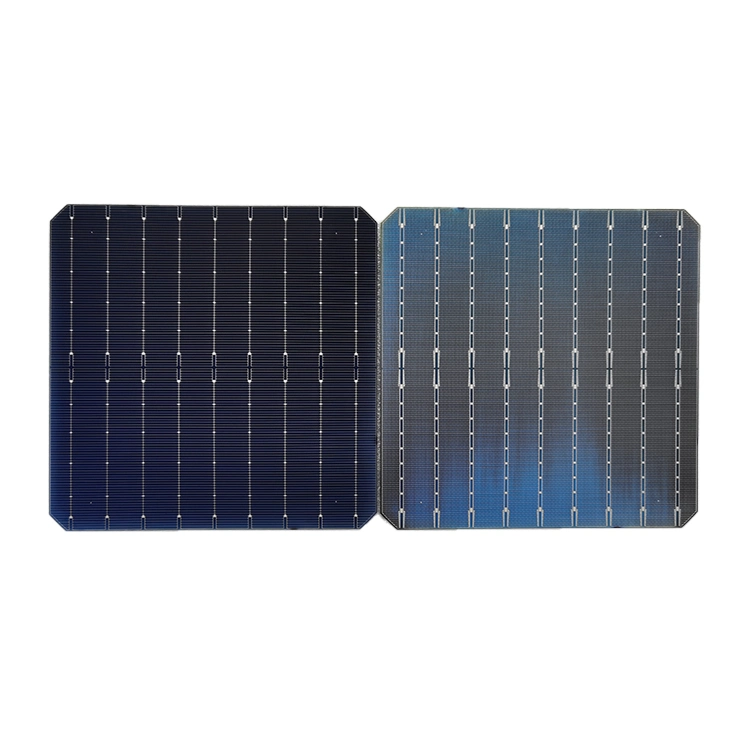
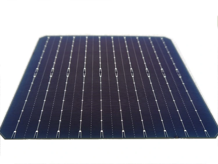
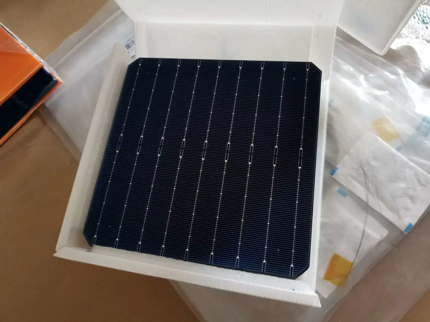
| Silicon type | size | Front electrode pattern |
| Mono-crystalline | 182*182±0.5Φ247mm | ten busbar |
| interval :17.3mm |
| Parameter items | | | Specification | Tolerance | Unit |
|
| Front surface | A | Finger quantity | 140 | - | - |
| | B | Front busbar width | 1 | ±0.1 | mm |
|
| | C | Distance between busbars | 17.3 | ±0.15 | mm |
|
| Rare surface | a | Back busbar width | 1.6 | ±0.3 | mm |
| | b | Distance between back busbars | 17.3 | ±0.15 | mm |
|
| | c | Back finger quantity | 160 | - | - |
|
| Eff (%) | Efficiency(%) | Pmpp(W) | Impp(A) | Umpp(V) | Isc(A) | Uoc(V) |
| 22.6 | 22.6-22.7 | 7.46 | 12.604 | 0.592 | 13.226 | 0.688 |
| 22.5 | 22.5-22.6 | 7.43 | 12.57 | 0.591 | 13.187 | 0.687 |
| 22.4 | 22.4-22.5 | 7.4 | 12.535 | 0.59 | 13.147 | 0.686 |
| 22.3 | 22.3-22.4 | 7.36 | 12.5 | 0.589 | 13.108 | 0.685 |
| 22.2 | 22.2-22.3 | 7.33 | 12.465 | 0.588 | 13.068 | 0.684 |
| 22.1 | 22.1-22.2 | 7.3 | 12.43 | 0.587 | 13.028 | 0.683 |
| 22 | 22.0-22.1 | 7.26 | 12.395 | 0.586 | 12.988 | 0.682 |
| 21 | 21.9-22.0 | 7.23 | 12.36 | 0.585 | 12.948 | 0.681 |
| Electrical properties | |
|
| Voc:-0.3 %/ºC | Intensity:1000 W/m² |
| Isc: +0.06 %/ºC | Spectrum:AM1.5G |
|
Production process
Cleaning & Texturing: Wafers are cleaned with industrial soaps and form square-based pyramids also called texture. The texturization helps to reduce the reflection of sunlight.
Diffusion: Wafers that have been pre-droped with boron during the casting process are then given a negative(n-type) surface characteristic by diffusing them with a phosphorus source at high temperature, which in turn creats the negative/positive(n-p) junction.
Etching: Phosphorus diffuses not only into the desired wafer surface but also into the side and the opposite surface to form PN. This gives a shunt path between the cell front and rear. Removal of the path around the wafer edge/edge junction isolation is named etching.
PECVD: By PECVD equipment, the wafers are coated with anti-reflection coating(ARC). It's the blue silicion nitride film to reduce reflection and promote absorption of light.
Printing & Heating: it was adopted by printing paste with screen technology to print the electrodes of silicion solar, and form a good ohmic contact.
Testing & Sorting: It means classifying the cells according to their efficiency tested under the simulated sunlight. Company Profile
Why choose us
Certifications
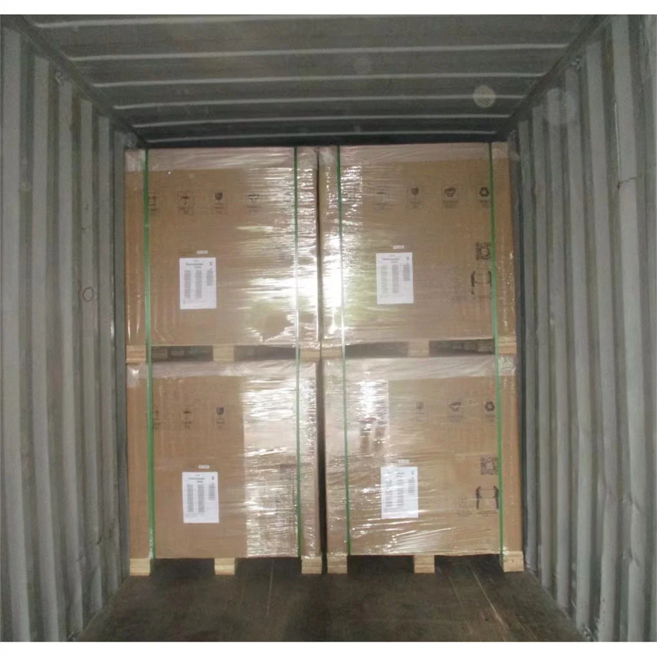
Packaging & Shipping
FAQ

 Complaint