
 Complaint

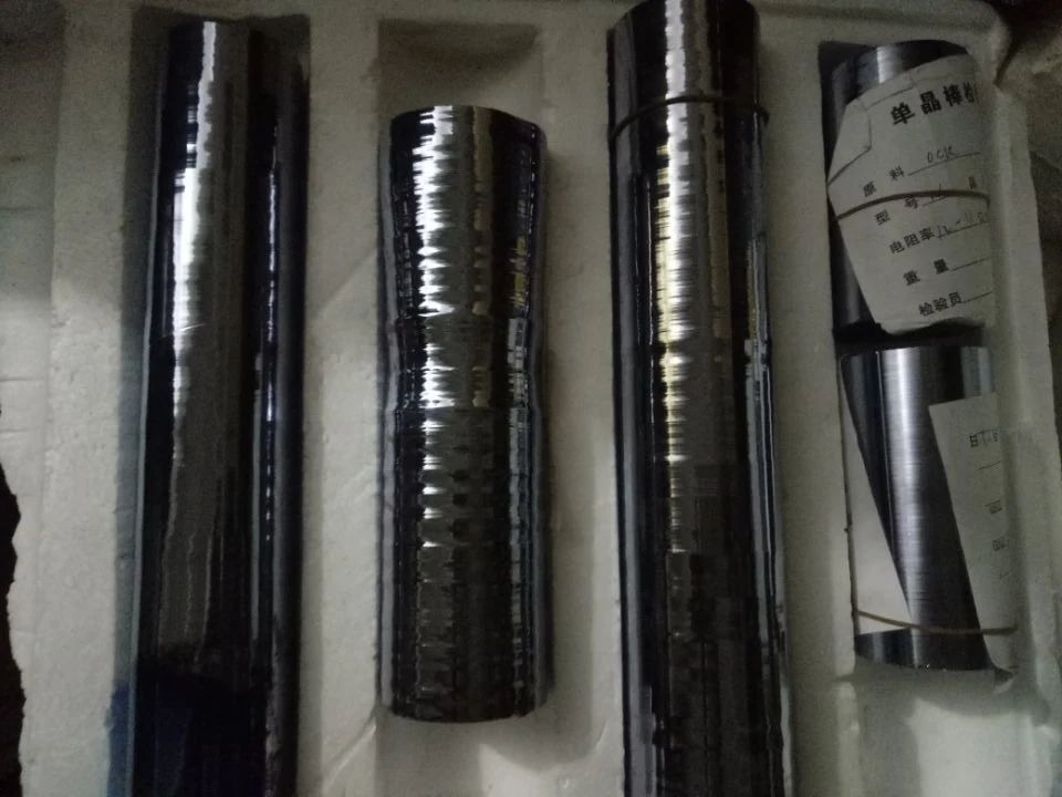
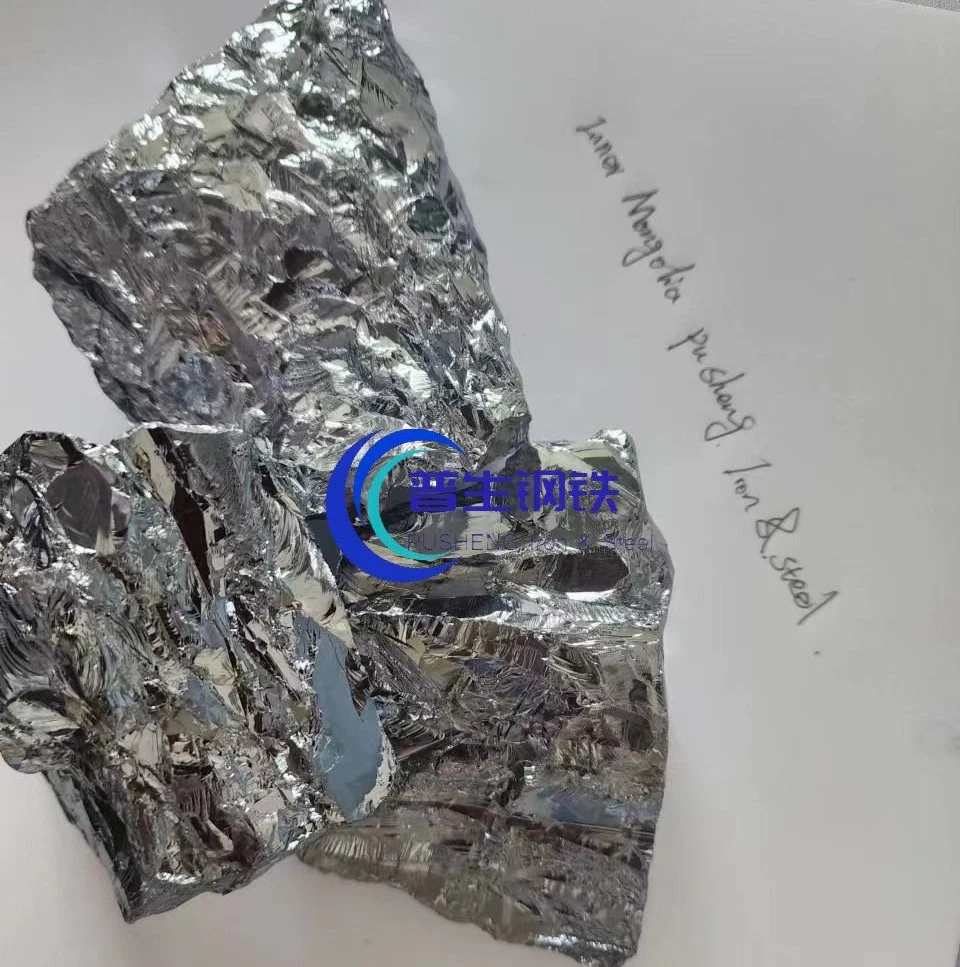
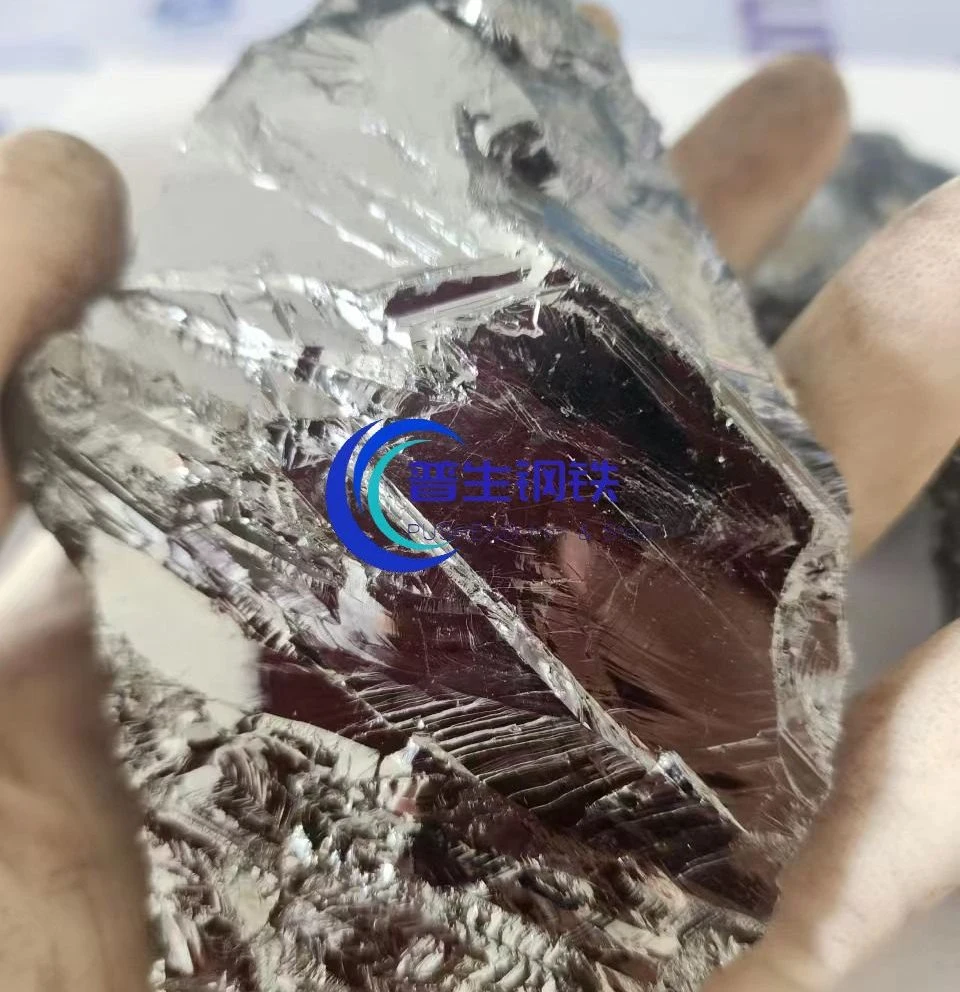
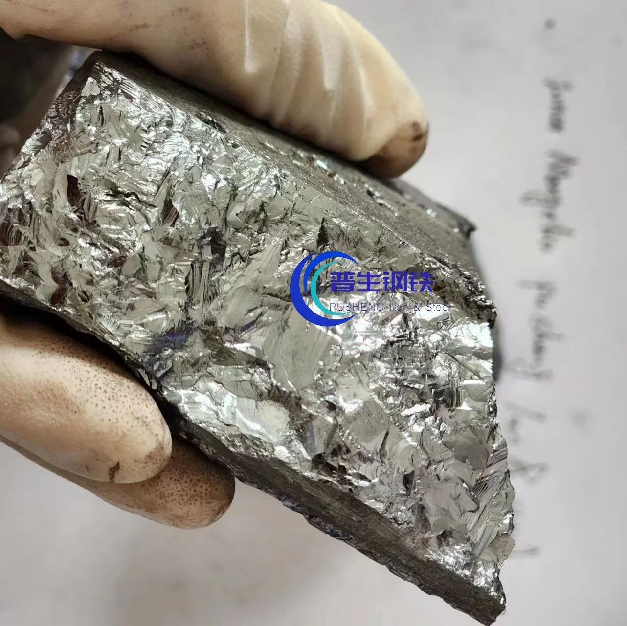
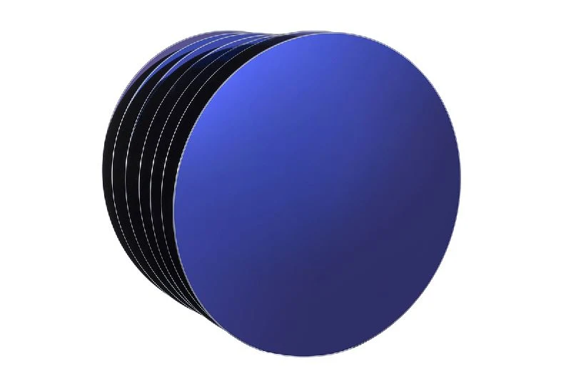
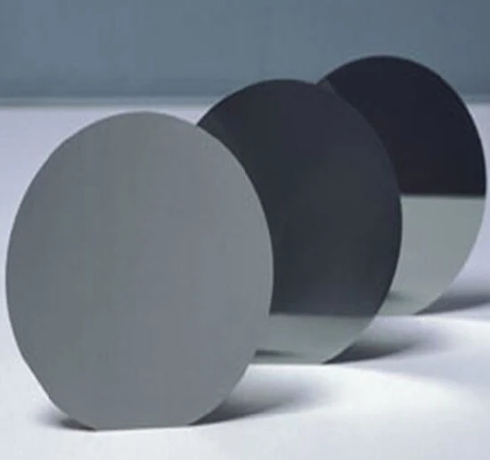
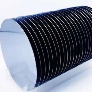
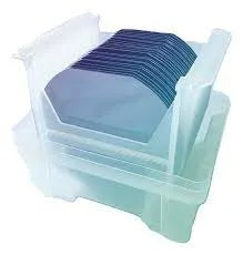
Silicon wafer: the sheet structure of single silicon material, with relatively thin thickness. There are mainly two kinds of structures, circular and square, including single crystal and polycrystalline. Single crystal is a kind of crystal material with fixed crystal orientation, which is generally used as the substrate of semiconductor integrated circuit and also used to make solar cell. Polycrystalline is a kind of crystal material without uniform fixed crystal orientation, which is generally used for solar photovoltaic power generation, or for the raw material of monocrystalline silicon. Monocrystalline silicon is a kind of excellent high-purity semiconductor material.
| Diameter | 2" | 3" | 4" | 5" | 6" | 8" | 12" |
| Grade | Prime Test Dummy | ||||||
| Growth Method | CZ | ||||||
| Orientation | < 1-0-0 > , < 1-1-1 > , < 1-1-0 > | ||||||
| Type/Dopant | P Type/Boron , N Type/Phos, N Type/As, N Type/Sb | ||||||
| Thickness (um) | 279 | 380 | 525 | 625 | 675 | 725 | 775 |
| Thickness Tolerance | Standard ± 25μm, Maximum Capabilities ± 5μm | ± 20μm | ± 20μm | ||||
| Resistivity | 0.001 - 100 ohm-cm | ||||||
| Surface Finished | P/E , P/P, E/E, G/G | ||||||
| TTV (um) | Standard < 10 um, Maximum Capabilities <5 um | ||||||
| Bow/Warp (um) | Standard <40 um, Maximum Capabilities <20 um | <40μm | <40μm | ||||
| Particle | <[email protected]; <[email protected]; <[email protected]; | ||||||
Seeopto Co., Ltd. is located in Pidu District, Chengdu. We aims to provide customers with professional design of laser crystal optical lenses, Coating service and all kinds of optical elements processing include YAG based crystals, YLF-based crystals, YVO4 based crystals, glass based laser Material, bonding crystals, silicon, germanium Infrared and semiconductor materials, LBO, BBO, KTP, ZGP Equal nonlinear material, Ti: Sapphire, CaF2, MgF2.optical sapphire customized components, window and aspheric lenses, powell lens and infrared materials products,etc.
We are also interested in discussing and manufacturing new material combinations and structural geometries. Our goal is to provide high-quality composite materials that can provide solutions to your system needs, so we encourage all design submissions. Please contact us for more information and technical support.
We can not only provide kinds of optical components, but also can make various types of optical coating such us Anti Reflection (AR) coating, High-Reflecting coating, Partial Reflection coating and Polarization Beamsplitter coating etc at single wavelength or broadband wavelength. Which can improve the transmission, high reflection. In addition such as Au, Si, Al, Ti metal coatings also is available.
Application of our items are very extensive and involves in mailitary project, aerospace, industry, scientific, medical instrument, photoelectric device, optical communication and mechanical equipment and so on. In the meantime we also cooperate with internal companies, we offer optics design and OEM service!
We constantly provide our clients with′ Quality products, excellent service, competitive prices and prompt delivery′ , sincerely welcome domestic and foreign customers to establish cooperation with us, creating a bright future in optical field!
What can we do for you ?
Seeopto Co., Ltd provide professional design of laser crystal optical lenses, Coating service and all kinds of optical elements processing We are also interested in discussing and manufacturing new material combinations and structural geometries.
Our goal is to provide high-quality composite materials that can provide solutions to your system needs, so we encourage all design submissions. Please contact us for more information and technical support.
Why choose Us ?
1. Reasonable quotation. We reject unrealistic low prices. As a prerequisite, to ensure the highest quality of Optical components and offer the reasonable price.
3. Timely Delivery. We will deliver the goods timely/promptly or deliver the goods in time.
4. Convenient logistics services. We usually cooperate with the famous express logistics company, including 90% regions of the world and ensure the products can delivery to the customers safety and quickly