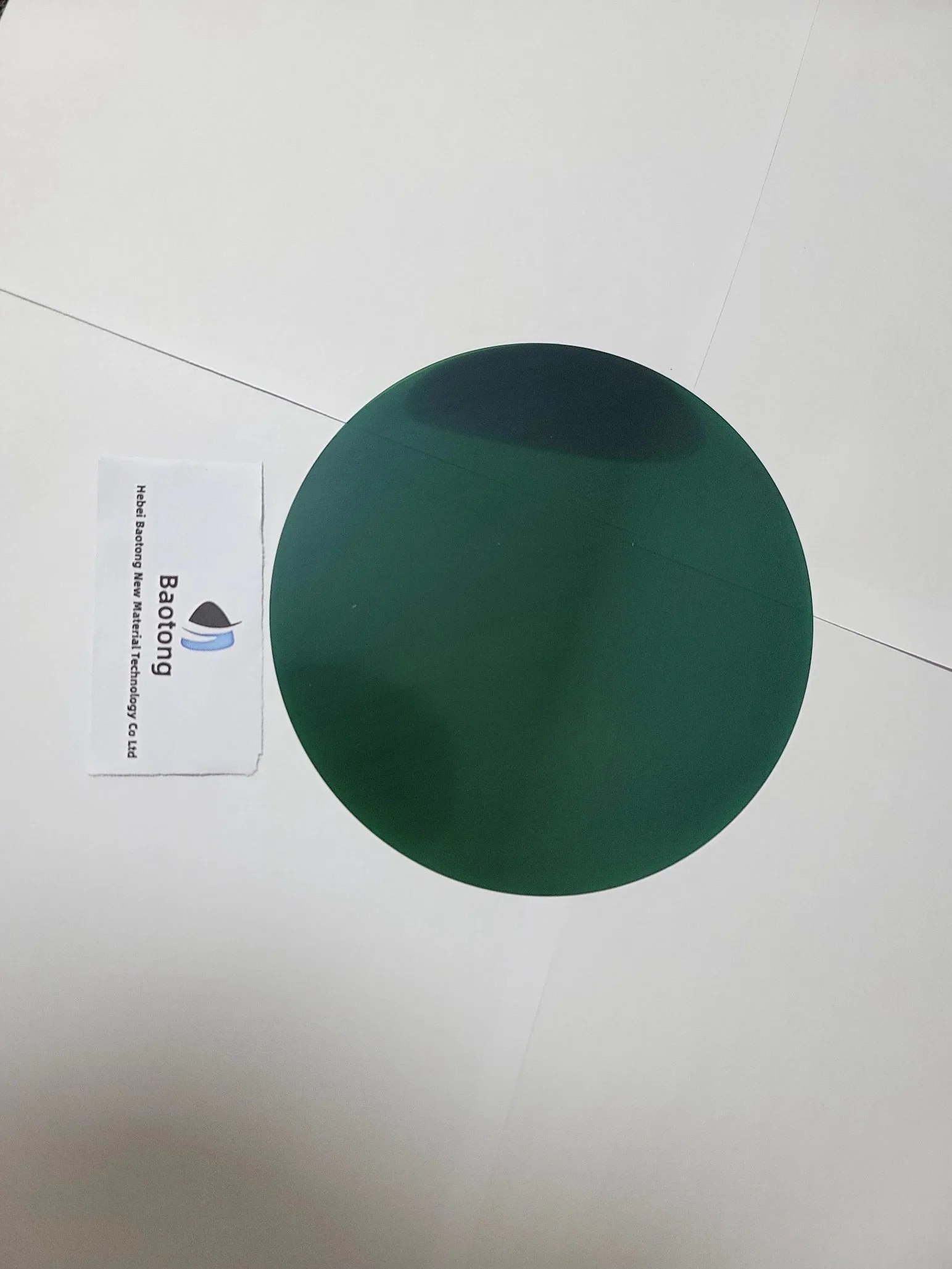
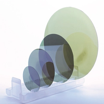
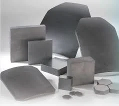
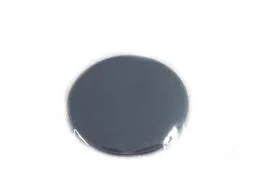
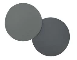
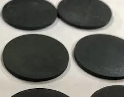
Silicon carbide (SiC) is a semiconductor containing silicon and carbon. SiC is used in semiconductor electronics devices that operate at high temperatures or high voltages, or both. Large single crystals of silicon carbide can be grown by the Lely method and they can be cut into gems known as synthetic moissanite.
Silicon Carbide SiC Specification
| Grade | Zero MPD | Production | Research Grade | Dummy Grade |
| Diameter | 50.8 ±0.38 mm, 76.2 ±0.38 mm, 100±0.5 mm, 150±0.25mm |
| Thickness | 4H-N | 350 μm±25μm |
| 4H-SI | 500 μm±25μm |
| Wafer Orientation | Off axis : 4.0° toward 1120 ±0.5° for 4H-N
On axis : <0001>±0.5° for 4H-SI |
| Micropipe Density | ≤1 cm-2 | ≤5 cm-2 | ≤15 cm-2 | ≤50 cm-2 |
| Resistivity | 4H-N | 0.015~0.028 Ω·cm |
| 6H-N | 0.02~0.1 Ω·cm |
| 4/6H-SI | >1E5 Ω·cm | (90%) >1E5 Ω·cm |
| Primary Flat | {10-10}±5.0° |
| Primary Flat Length | 15.9 mm±1.7 mm, 22.2 mm±3.2 mm, 32.5 mm±2.0 mm, 47.5 mm±2.5 mm |
| Secondary Flat Length | 8.0 mm±1.7 mm, 11.2 mm±1.5 mm, 18.0mm±2.0 mm, -----, |
| Secondary Flat Orientation | Silicon face up: 90° CW. from Prime flat ±5.0° |
| Edge exclusion | 3 mm |
| TTV/Bow /Warp | ≤15μm /≤25μm /≤40μm |
| Roughness | Polish Ra≤1 nm |
| CMP Ra≤0.5 nm |
| Cracks by high intensity light | None | None | 1 allowed, ≤1 mm |
| Hex Plates by high intensity light | Cumulative area≤1 % | Cumulative area≤1 % | Cumulative area≤3 % |
| Polytype Areas by high intensity light | None | Cumulative area≤2 % | Cumulative area≤5% |
Scratches by
high intensity light | 3 scratches to 1×
wafer diameter
cumulative length | 5 scratches to 1×
wafer diameter
cumulative length | 8 scratches to 1×
wafer diameter
cumulative length |
| Edge chip | None | 3 allowed, ≤0.5 mm each | 5 allowed, ≤1 mm each |
Contamination by
high intensity light | None |
Silicon carbide has the advantages of high thermal conductivity (3 times higher than silicon) and small lattice mismatch with gallium nitride (4%), which makes it suitable for use as a new generation of light-emitting diode (LED) substrate. It is no exaggeration to say that silicon carbide has become the leading edge and commanding height of the global semiconductor industry. On the whole, the complete industry chain of silicon carbide semiconductor includes: silicon carbide raw materials - ingot - chip - epitaxial - chip - device - module. In the process of LED preparation, the upstream silicon carbide chip (substrate) material is the main factor that determines the performance indexes such as LED color, brightness and life.
The substrate material is the basis for the growth of gallium nitride epitaxial film and the main component of LED devices. The surface roughness, thermal expansion coefficient, thermal conductivity coefficient and lattice matching degree between substrate and epitaxial material have a profound influence on the luminous efficiency and stability of high brightness LED.
At present, the common substrate materials are sapphire (Al2O3), monocrystalline silicon and silicon carbide. Silicon carbide has a variety of crystal types, which can be divided into three categories: cubic (such as 3c-sic), hexagonal (such as 4h-sic) and diamond (such as 15r-sic), of which 4h-sic and 6h-sic are mainly used as gallium nitride substrates.
By comparing with sapphire and monocrystalline silicon, we can see how the sic substrate is favored by researchers and becomes the high-end variety of substrate materials. Lattice mismatch and thermal mismatch. The lattice mismatch rate of sapphire is 13.9%, that of silicon is 16.9%, and that of silicon carbide is only 3.4%. In terms of thermal mismatch rate, sapphire is in the middle of 30.3%, and monocrystalline silicon has the highest thermal mismatch rate, reaching 53.48837%.
In the process of growing gallium nitride on monocrystalline silicon substrate, researchers found that its thin film would be subjected to huge thermal stress, resulting in a large number of defects and even cracks in the epitaxial layer. Therefore, it is difficult to grow high quality gallium nitride films on silicon substrates. However, the thermal mismatch rate of 6h-sic was only 15.92129%. Therefore, in terms of crystal structure characteristics, the crystal structure of 4h-sic and 6h-sic and gallium nitride are wurtzite structures, with the lowest lattice mismatch rate and thermal mismatch rate, which is most suitable for the growth of high-quality gallium nitride epitaxial layer.
Electrical conductivity.
Sapphire is an insulator, in which case it is impossible to make devices of vertical structure, and usually only n-type and p-type electrodes are made on the outer surface of the epitaxial layer. Silicon carbide and monocrystalline silicon have good electrical conductivity, which can be used to make vertical LED. Compared with the horizontal device prepared on sapphire substrate, the process of preparing vertical device on silicon carbide is simple. The leds of the two structures are shown in figure 2 and figure 3. Because the conductive substrate is used as the lower electrode, the device has only one electrode on the upper surface, which increases the luminous area. In addition, the vertical LED has a more uniform current distribution density, which avoids the local overheating caused by the uneven current density distribution of the horizontal structure, and can carry a higher positive current.
Figure 2 horizontal structure LED (picture source: research progress of gan-based LED substrate material)
Figure 3 vertical structure LED (picture source: research progress of gan-based LED substrate materials) Thermal conductivity.
Sapphire has poor heat dissipation performance, only 0.3 W·cm-1· k-1 at 300K, and 1.3w ·cm-1· k-1 thermal conductivity of single crystal silicon at 300K, both of which are far lower than the thermal conductivity of silicon carbide crystal. In addition, the vertical LED made of silicon carbide is better than the horizontal LED made of sapphire, the heat generated can be exported from both ends of the electrode, so it is more suitable for the substrate material of high-power LED, and has a longer service life.
Optical properties.
Sapphire and silicon carbide do not absorb visible light, the absorption of silicon substrate to light is serious, LED light efficiency is low. However, the sic substrate is not omnipotent, its biggest problem is the chip production problem. Sapphire is currently the most widely used commercial LED substrate material, sapphire by the melt method to grow, more mature process, can obtain a low cost, large size, high quality single crystal, suitable for industrial development.
Similarly, monocrystalline silicon growth technology is highly mature, making it easy to obtain low-cost, large size (6-12 inches), high-quality substrates, which can significantly reduce the cost of Leds. However, it is difficult to grow high quality and large size silicon carbide single crystal, and the layered structure of silicon carbide is easy to cleavage, poor processing performance, it is easy to introduce stepped defects on the substrate surface, affecting the quality of the epitaxial layer. The price of silicon carbide substrate of the same size is dozens of times that of sapphire substrate.
In general, the lattice mismatches and thermal mismatches between silicon carbide crystals and gallium nitride are low, and high quality gallium nitride films can be grown. Excellent electrical conductivity, can be made into vertical LED structure; Good thermal conductivity, long service life, suitable for high-power LED production; Excellent optical performance, no absorption of visible light, high efficiency. However, although silicon carbide crystals are very suitable for use as LED substrate materials, their cost is high, and their related technologies and patents face international monopoly, which is an urgent problem to be solved in the future.
Seeopto Co., Ltd. is located in Pidu District, Chengdu. We aims to provide customers with professional design of laser crystal optical lenses, Coating service and all kinds of optical elements processing include YAG based crystals, YLF-based crystals, YVO4 based crystals, glass based laser Material, bonding crystals, silicon, germanium Infrared and semiconductor materials, LBO, BBO, KTP, ZGP Equal nonlinear material, Ti: Sapphire, CaF2, MgF2.optical sapphire customized components, window and aspheric lenses, powell lens and infrared materials products,etc.
We are also interested in discussing and manufacturing new material combinations and structural geometries. Our goal is to provide high-quality composite materials that can provide solutions to your system needs, so we encourage all design submissions. Please contact us for more information and technical support.
We can not only provide kinds of optical components, but also can make various types of optical coating such us Anti Reflection (AR) coating, High-Reflecting coating, Partial Reflection coating and Polarization Beamsplitter coating etc at single wavelength or broadband wavelength. Which can improve the transmission, high reflection. In addition such as Au, Si, Al, Ti metal coatings also is available.
Application of our items are very extensive and involves in mailitary project, aerospace, industry, scientific, medical instrument, photoelectric device, optical communication and mechanical equipment and so on. In the meantime we also cooperate with internal companies, we offer optics design and OEM service!
We constantly provide our clients with′ Quality products, excellent service, competitive prices and prompt delivery′ , sincerely welcome domestic and foreign customers to establish cooperation with us, creating a bright future in optical field!
What can we do for you ?
Seeopto Co., Ltd provide professional design of laser crystal optical lenses, Coating service and all kinds of optical elements processing We are also interested in discussing and manufacturing new material combinations and structural geometries.
Our goal is to provide high-quality composite materials that can provide solutions to your system needs, so we encourage all design submissions. Please contact us for more information and technical support.
Why choose Us ?
1. Reasonable quotation. We reject unrealistic low prices. As a prerequisite, to ensure the highest quality of Optical components and offer the reasonable price.
3. Timely Delivery. We will deliver the goods timely/promptly or deliver the goods in time.
4. Convenient logistics services. We usually cooperate with the famous express logistics company, including 90% regions of the world and ensure the products can delivery to the customers safety and quickly
 Complaint