 Complaint

| XRD-FWHM | 002 | 102 |
| 3-4μm GaN/Sapphire | 200-300 | 250-450 |
| Item | GaN-FS-C-U-C50 | GaN-FS-C-N-C50 | GaN-FS-C-SI-C50 |
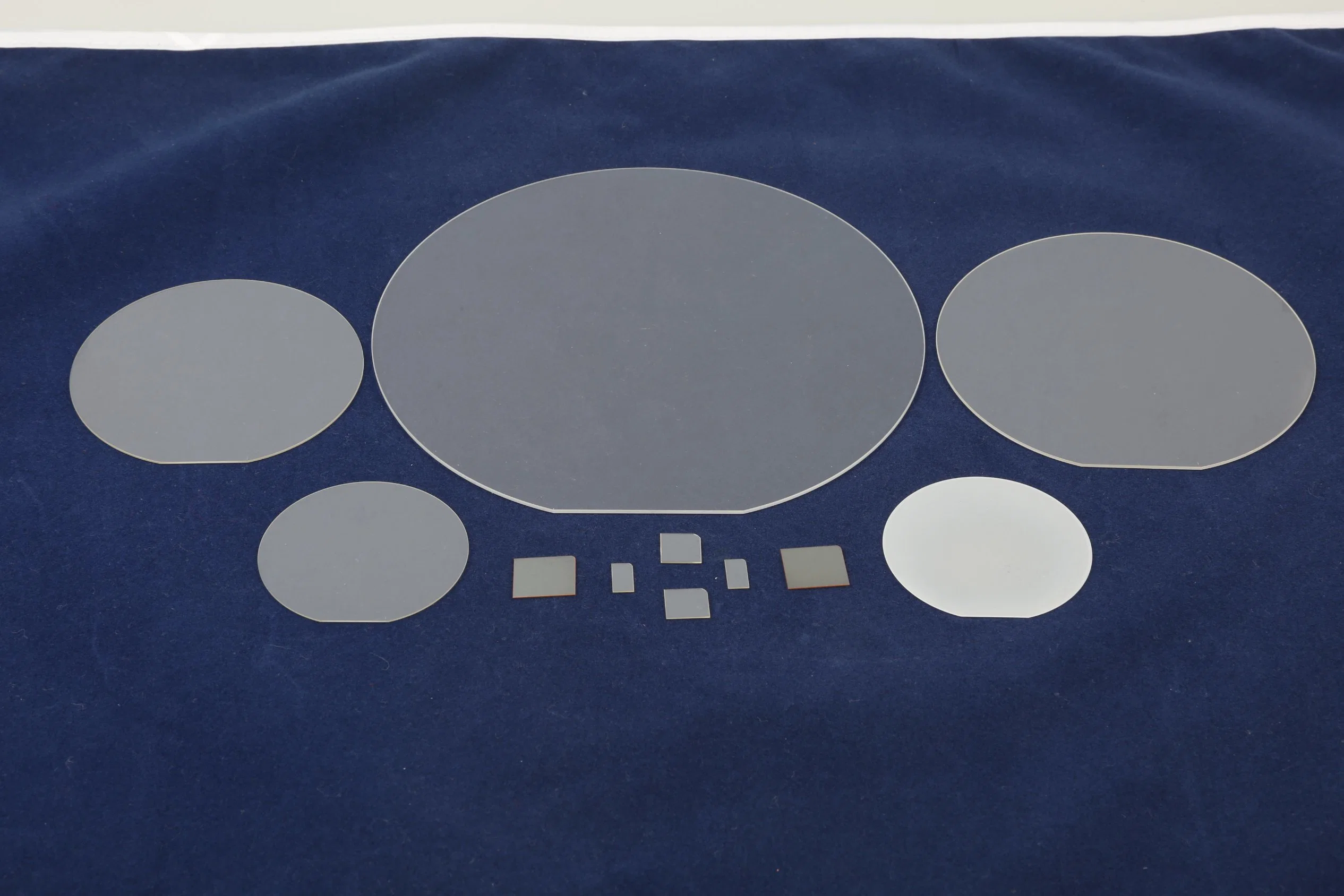
| Dimensions | Ф 50.8 mm ± 1 mm | ||
| Thickness | 350 ± 25 µm | ||
| Useable Surface Area | > 90% | ||
| Orientation | C-plane (0001) off angle toward M-Axis 0.35°± 0.15° | ||
| Orientation Flat | (1-100) ± 0.5°, 16.0 ± 1.0 mm | ||
| Secondary Orientation Flat | (11-20) ± 3°, 8.0 ± 1.0 mm | ||
| Total Thickness Variation | ≤ 15 µm | ||
| BOW | ≤ 20 µm | ||
| Conduction Type | N-type (Undoped) | N-type (Ge-doped) | Semi-Insulating (Fe-doped) |
| Resistivity(300K) | < 0.5 Ω·cm | < 0.05 Ω·cm | >106 Ω·cm |
| Dislocation Density | 1~9x105 cm-2 | 5x105 cm-2 ~3x106 cm-2 | 1~9x105 cm-2 |
| 1~3x106 cm-2 | 1~3x106 cm-2 | ||
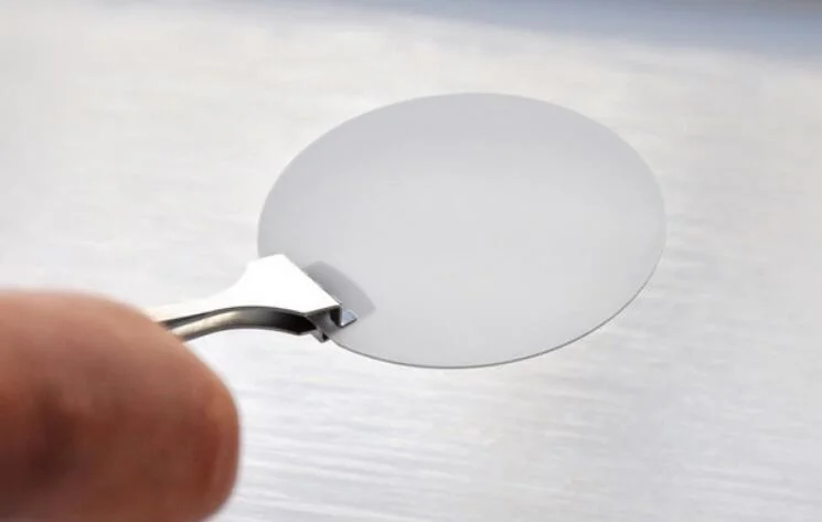
| Polishing | Front Surface: Ra < 0.2 nm. Epi-ready polished Back Surface: Fine ground | ||
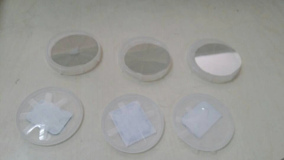
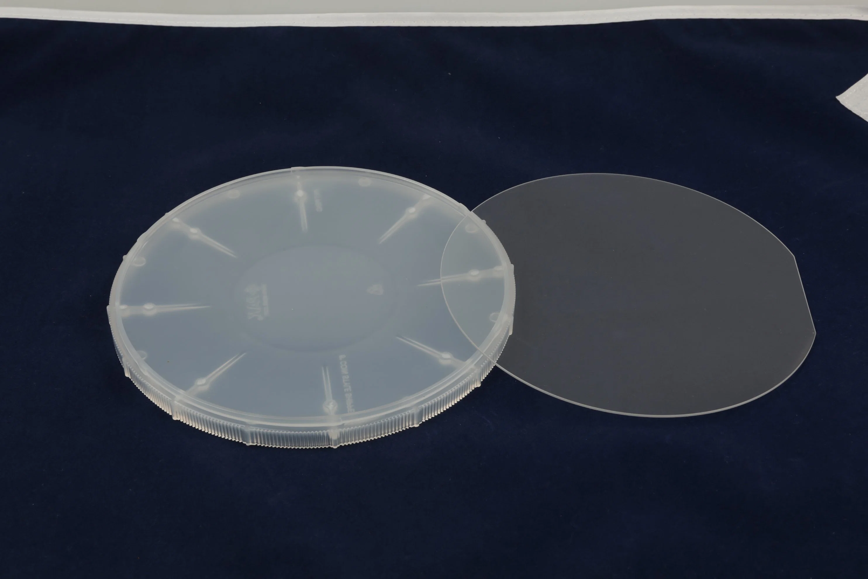
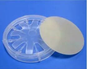
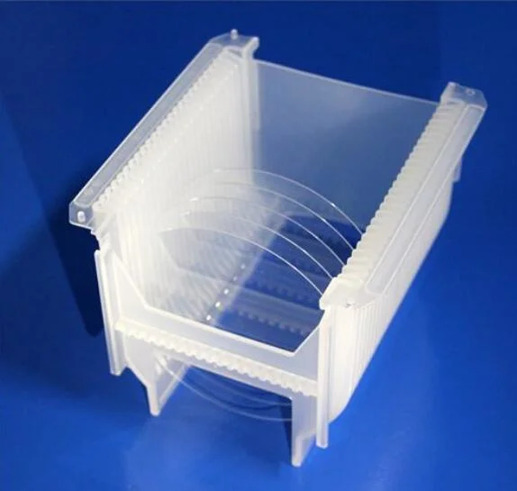
| Package | Packaged in a class 100 clean room environment, in single wafer containers, under a nitrogen atmosphere. | ||
| Item | GaN-T-C-U-C100 | GaN-T-C-N-C100 |
| Dimensions | Ф 100 mm ± 0.1 mm | |
| Thickness | 4 µm, 20 µm | |
| Orientation | C-plane(0001) ± 0.5° | |
| Conduction Type | N-type (Undoped) | N-type (Si-doped) |
| Resistivity 300K | < 0.5 Ω·cm | < 0.05 Ω·cm |
| Carrier Concentration | < 5x1017 cm-3 | > 1x1018 cm-3 |
| Mobility | ~ 300cm2/V·s | ~ 200 cm2/V·s |
| Dislocation Density | Less than 5x108 cm-2 | |
| Substrate structure | GaN on Sapphire(Standard: SSP Option: DSP) | |
| Useable Surface Area | > 90% | |
| Package | Packaged in a class 100 clean room environment, in cassettes of 25pcs or single wafer containers, under a nitrogen atmosphere. | |