 Complaint

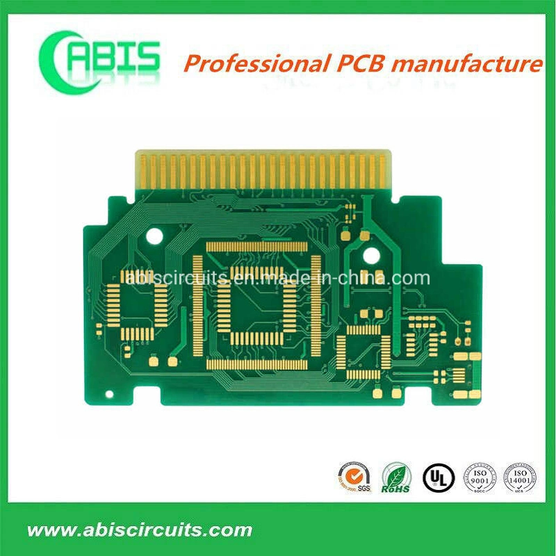
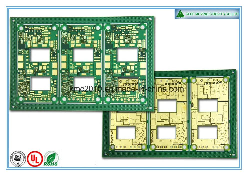
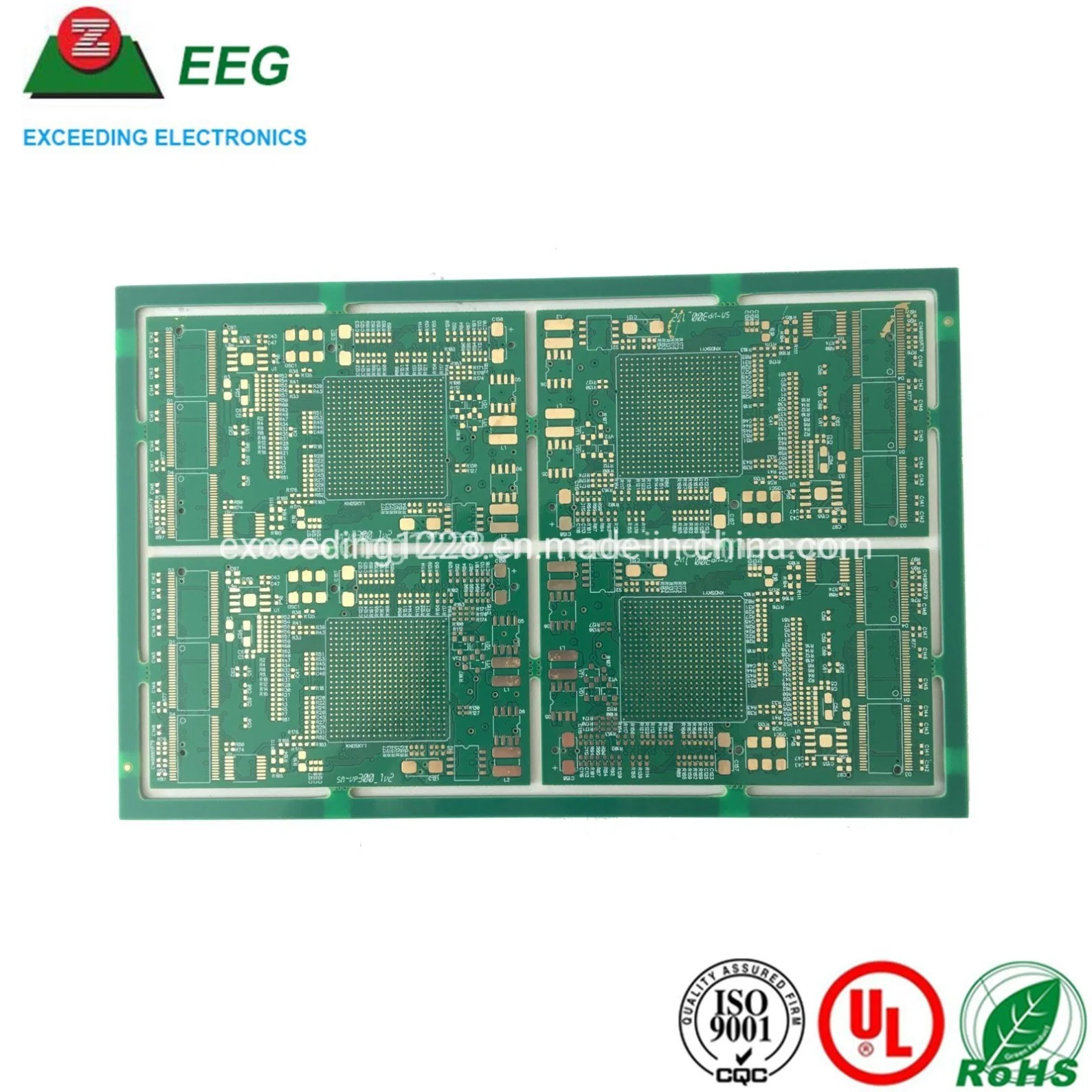
| Technical Capabilities | |||
| Items | Speci. | Remark | |
| Max panel size | 32" x 20.5"(800mm x 520mm) | ||
| Max. Board size | 2000×610mm | ||
Min. board Thickness | 2-layer 0.15mm | ||
| 4-layer 0.4mm | |||
| 6-layer 0.6mm | |||
| 8-layer 1.5mm | |||
| 10-layer 1.6~2.0mm | |||
| Min. line Width/Space | 0.1mm(4mil) | ||
| Max. Copper thickness | 10OZ | ||
| Min. S/M Pitch | 0.1mm(4mil) | ||
| Min. hole size | 0.2mm(8mil) | ||
| Hole dia. Tolerance (PTH) | ±0.05mm(2mil) | ||
| Hole dia. Tolerance | ,+0/-0.05mm(2mil) | ||
| Hole position deviation | ±0.05mm(2mil) | ||
| Outline tolerance | ±0.10mm(4mil) | ||
| Twist & Bent | 0.75% | ||
| Insulation Resistance | >10 12 Ω Normal | ||
| Electric strength | >1.3kv/mm | ||
| S/M abrasion | >6H | ||
| Thermal stress | 288°C 10Sec | ||
| Test Voltage | 50-300V | ||
| Min. blind/buried via | 0.15mm (6mil) | ||
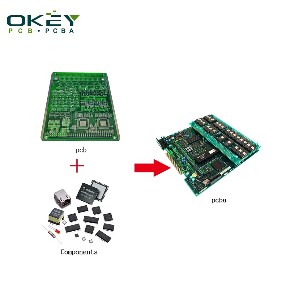
Surface Finished | HASL, ENIG, ImAg, Imsn OSP, Plating AG, Plating gold | ||
Materials | FR4,H- TG,Teflon,Rogers,Ceramics,Aluminium, Copper base | ||
| Min trace width/ space (inner layer) | 4mil/4mil(0.1mm/0.1mm) | ||
| Min PAD (inner layer) | 5 mil(0.13mm) | hole ring width | |
| Min thickness(inner layer) | 4 mil(0.1mm) | without copper | |
| Inner copper thickness | 1~4 oz | ||
| Outer copper thickness | 0.5~6 oz | ||
| Finished board thickness | 0.4-3.2 mm | ||
Board thickness tolerance control | ±0.10 mm | ±0.10 mm | 1~4 L |
| ±10% | ±10% | 6~8 L | |
| ±10% | ±10% | ≥10 L | |
| Inner layer treatment | brown oxidation | ||
| Layer count Capability | 1-30 LAYER | ||
| alignment between ML | ±2mil | ||
| Min drilling | 0.15 mm | ||
| Min finished hole | 0.1 mm | ||
| NO | Item | Technical capabilities |
| 1 | Layers | 1-12 layers |
| 2 | Max. Board size | 2000×610mm |
| 3 | Min. board Thickness | 2-layer 0.25mm |
| 4-layer 0.6mm | ||
| 6-layer 0.8mm | ||
| 8-layer 1.5mm | ||
| 10-layer 1.6~2.0mm | ||
| 4 | Min. line Width/Space | 0.15mm(4-5mil) |
| 5 | Max. Copper thickness | 10OZ |
| 6 | Min. S/M Pitch | 0.15mm(4-5mil) |
| 7 | Min. hole size | 0.2mm(8mil) |
| 8 | Hole dia. Tolerance (PTH) | ±0.05mm(2mil) |
| 9 | Hole dia. Tolerance (NPTH) | +0/-0.05mm(2mil) |
| 10 | Hole position deviation | ±0.05mm(2mil) |
| 11 | Outline tolerance | ±0.10mm(4mil) |
| 12 | Twist & Bent | 0.75% |
| 13 | Insulation Resistance | >10 12 Ω Normal |
| 14 | Electric strength | >1.3kv/mm |
| 15 | S/M abrasion | >6H |
| 16 | Thermal stress | 288°C10Sec |
| 17 | Test Voltage | 50-300V |
| 18 | Min. blind/buried via | 0.2mm (8mil) |
| 19 | Surface Finished | HAL, ENIG, ImAg, Imsn OSP, Plating AG, Plating gold |
| 20 | Materials | FR4,H-TG,Teflon,Rogers,Ceramics,Aluminium, Copper base |