

 Complaint

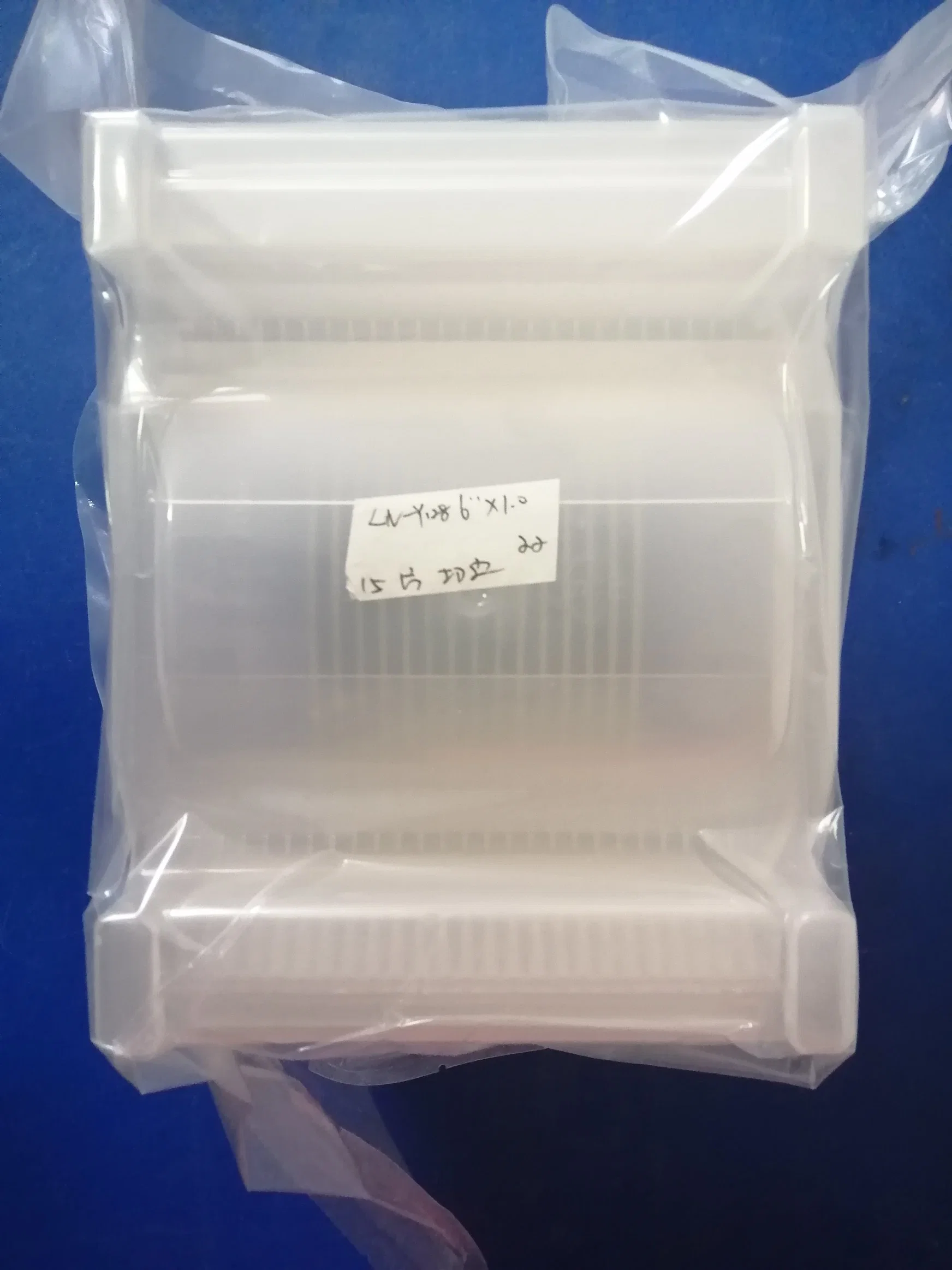
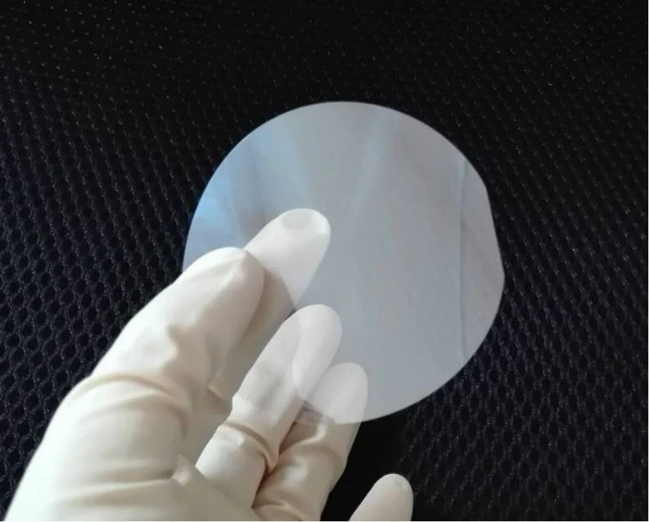
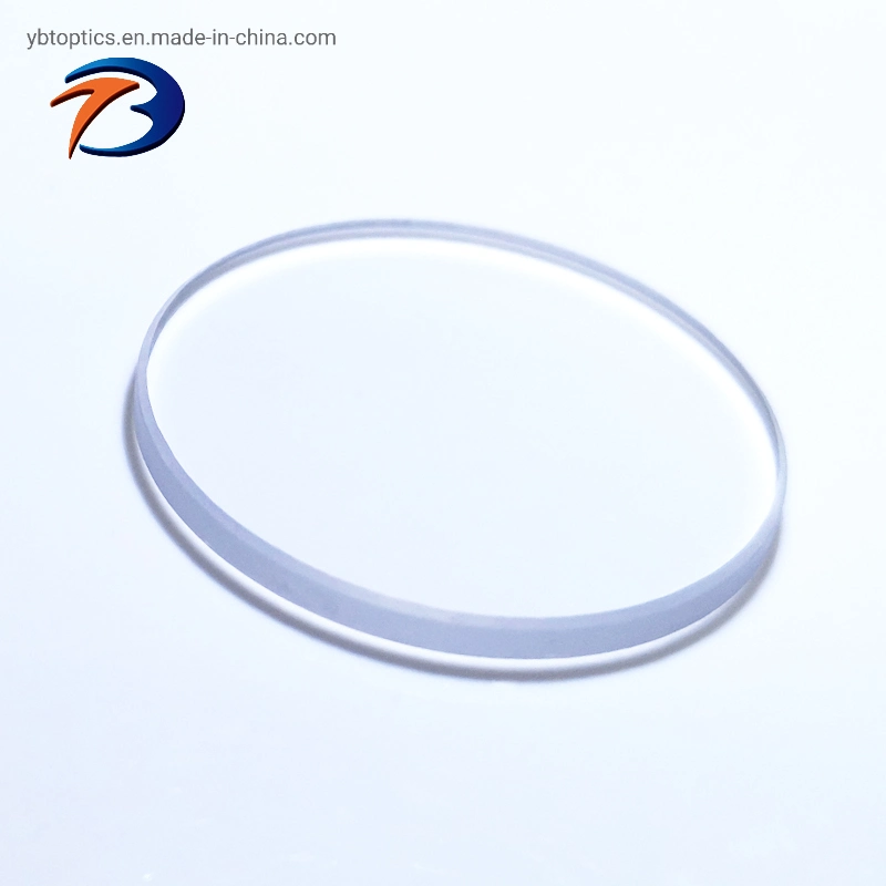
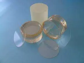
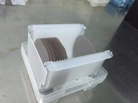
Lithium Niobate (LiNbO3) Wafer (2inch-6inch)
LiNbO3 is a ferroelectric material with variety of applications.
A great variety of devices has been developed based upon this material having unique electro-optical, photoelastic, piezo-electric and non-linear properties combined with good mechanical and chemical stability and wide transparency range. For instance, in optical modulation and Q-switching large electro-optic coefficients of lithium niobate infrared wavelengths is used. By-turn, the large nonlinear (d) coefficient of LiNbO3 allows very successfully use this material in optical parametric oscillaton and difference frequency mixing to generate tunable infrared wavelengths and second harmonic.
It is widely used as frequency doublers for wavelength over 1 micron and optical parametric oscillators (OPOs) pumped at 1064 nm as well as quasi-phase-matched (QPM) devices.
LiNbO3 is also one of the most attractive materials for optoelectronics. A great variety of devices has been developed based upon this material having unique electro-optical, photoelastic, piezo-electric and non-linear properties combined with good mechanical and chemical stability and wide transparency range.
Surface acoustic wave filter, isolator, narrow-band filter, sensor, the photon tunable filter, acousto-optic device, Optical gyroscope, optical waveguide, photoswitch, light modulation direction coupler, Optical modulator, Interferometer gyrator, High-speed long-distance communication devices and double-frequency device.
The Application of SAW devices are especially used in mobile phones as dielectric filters band-pass filter, RF filter and IF filter. broadband filters, include radar technology, remote controls for home electronics
| Orientation | X-Axis, Y-Axis, Z-Axis, Y-Axis 128°/64°/41°/36° Rotated |
| Orientation Tolerance | ±0.2° |
| Diameter | 50.8±0.1mm (2 inches), 76.2±0.2mm (3 inches), 100±0.3mm (4 inches), 150±0.5mm (6 inches) |
| Thickness | 500±25µm, 660±25µm, 710±25µm, 790±25µm, 1000±25µm |
| Primary Flat Length | 16.0±1.5mm, 22.0±2.0mm, 32.5±2.5mm |
| TTV | ≤30µm |
| BOW | ≤30µm |
| Front Surface | Ra < 1nm |
| Back Surface | Fine ground or polished (Ra<1nm) |
optical grade quality wafers
Saw grade quality wafers
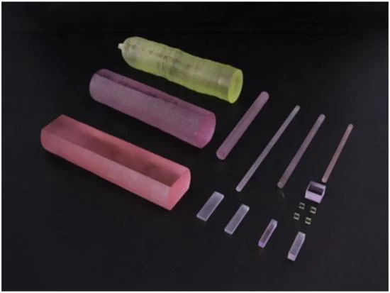
MgO doped LiNbO3
Fe doped LiNbO3
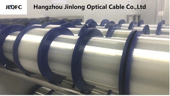
Innovation point: Through the growth equipment modification,we create simulation of crystal growth system and can design crystal shape. The computer chip control the changing of crystal shape according to crystal growth status, through the processing of precision sensor signals. We self-design a set of graded composite temperature structure. With the help of it, the temperature gradient in crystals, melt and the solid liquid interface reach the good state for optical crystal growth.
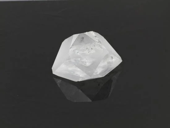
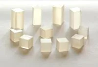
Fe Dopped LN ingot
Ingot and wafers