

 Complaint

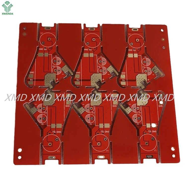
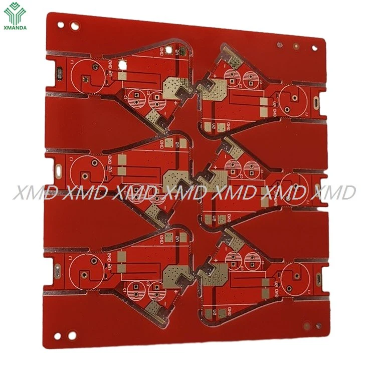
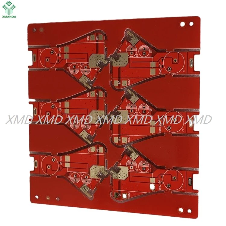
Specifications:
Features:
1. The integration of the board design is very high, the thickness-to-diameter ratio exceeds 10:1, and the difficulty of electroplating of copper is high.
2. Made of TG140 material
Shenzhen XMD Circuits Co.,Ltd, previously known as Jaleny(jlypcb), was founded in 2009 and started the journey of circuit board in Shenzhen,China. Through the introduction of advanced production and testing equipment and technical exchanges with factories in the same industry and engineering colleges, XMD greatly expanded the process capacity of double-sided board and multi-layer board. In 2011, we began to explore overseas markets and export foreign orders to all parts of the world. In 2018, Jiangxi Ji'an added a new production line, mainly making batch orders.
Able to produce 50,000 sqm of PCBs monthly
One-stop solutions for clients (PCB & PCBA)
Over 12 years of Experience in PCBs
Avg Response time: ≤24 h (experienced Engineers to Serve you)
Comply with RoHS,TS16949,ISO9001 and UL certifications.
Flexibilities in Shipment Arrangement (FOB HK or Shenzhen by sea or by air, CIF via DHL,Fedex,UPS or TNT etc.)
A professional team, using automation, digitization to greatly improve pcb production efficiency and reduce PCB procurement costs.
| Our Capabilities and Technology | |||
| Items | 2022 | 2023 | |
| Layers | (MP):22layer,(Sampling):32 layer | (MP):32layer | |
| Max. Board THK | Sampling 4.0mm / MP :3.2mm | Sampling 5.0mm / MP:3.2mm | |
| Min. Board THK | Sampling :0.4mm /MP :0.5mm | Sampling: 0.3mm / MP:0.4mm | |
| Base copper | Inner layer | 1/3 ~ 6OZ | 1/3~8 OZ |
| Outer layer | 1/3 ~ 6 OZ | 1/3 ~ 8 OZ | |
| Borehole diameter | Min.PTH | 0.2mm | 0.15mm |
| Max. aspect ratio | 10:01 | 12:01 | |
| HDI aspect ratio | 0.8:1 | 1:01 | |
| Tolerances | PTH | ±0.076mm | ±0.05mm |
| NPTH | ±0.05mm | ±0.03mm | |
| Solder mask opening | 0.05mm | 0.03mm | |
| Solder dam | (Green) 0.076mm , | (Green) 0.076mm , | |
| (other color) 0.1mm | (other color) 0.08mm | ||
| Min. core THK. | 0.1mm | 0.08mm | |
| Bow&twist | ≤0.5% | ≤0.5% | |
| Routing Tol. | Sampling :±0.075mm /MP:±0.1mm | Sampling:±0.075mm /MP:±0.075mm | |
| Impedance Tol. | ±10% | ±8% | |
| Min. w/s (Inner layer) | 0.075 / 0.075mm | 0.075 / 0.075mm | |
| Min. w/s (Outer layer) | 0.075 / 0.075mm | 0.075 / 0.075mm | |
| (Min. BGA size) | 0.2mm | 0.15mm | |
| (pitch)(Min. BGA Pitch) | 0.65mm | 0.5mm | |
| (Working panel size) | 600mm*700mm | 600mm*700mm | |
| Special process | Split gold fingers, Counter-bore , Counter-sink, Back-Drill, POFV , Mech. Drilling Blind hole. | ||