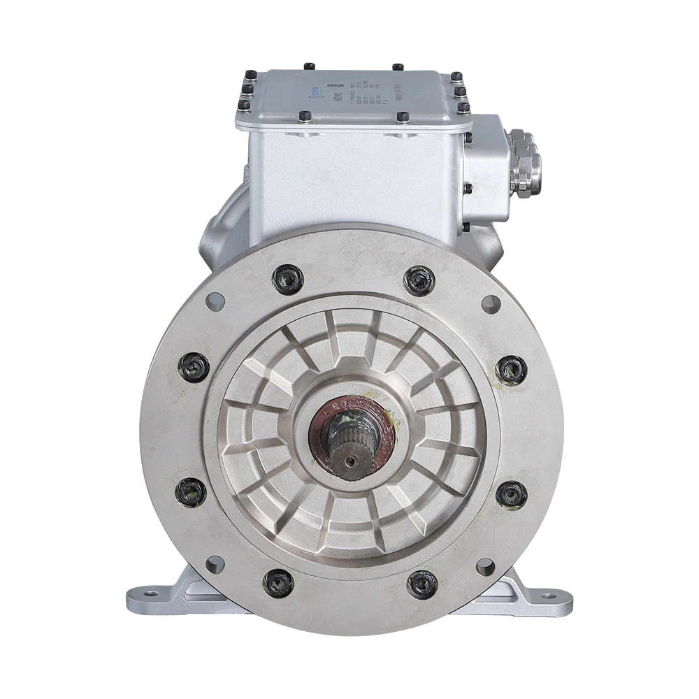


 Complaint

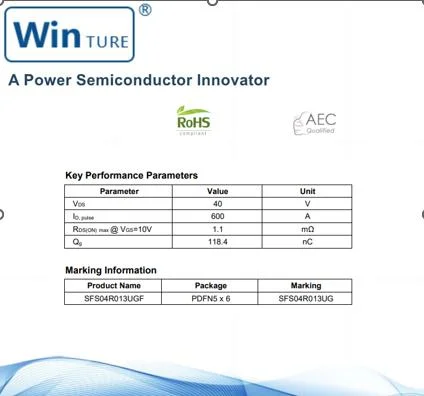
| Parameter | Value | Unit |
| VDS | 40 | V |
| ID, pulse | 600 | A |
| RDS(ON) max @ VGS=10V | 1.1 | mΩ |
| Qg | 118.4 | nC |
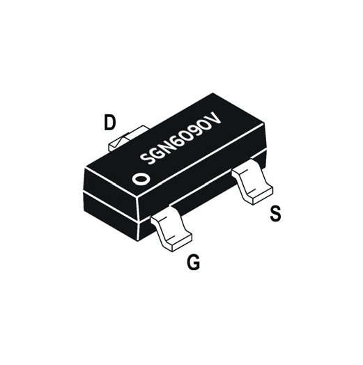
| Product Name | Package | Marking |
| SFS04R013UGF | PDFN5 x 6 | SFS04R013UG |
| Parameter | Symbol | Value | Unit |
| Drain source voltage | VDS | 40 | V |
| Gate source voltage | VGS | ±20 | V |
| Continuous drain current1), TC=25 °C | ID | 200 | A |
| Pulsed drain current2), TC=25 °C | ID, pulse | 600 | A |
| Continuous diode forward current1), TC=25 °C | IS | 200 | A |
| Diode pulsed current2), TC=25 °C | IS, Pulse | 600 | A |
| Power dissipation3), TC=25 °C | PD | 178 | W |
| Single pulsed avalanche energy5) | EAS | 144 | mJ |
| Operation and storage temperature | Tstg,Tj | -55 to 175 | °C |
| Parameter | Symbol | Value | Unit |
| Thermal resistance, junction-case | RθJC | 0.84 | °C/W |
| Thermal resistance, junction-ambient4) | RθJA | 62 | °C/W |
| Parameter | Symbol | Min. | Typ. | Max. | Unit | Test condition |
| Drain-source breakdown voltage | BVDSS | 40 | V | VGS=0 V, ID=250 μA | ||
| Gate threshold voltage | VGS(th) | 1.2 | 2.5 | V | VDS=VGS, ID=250 μA | |
| Drain-source on- state resistance | RDS(ON) | 0.9 | 1.1 | mΩ | VGS=10 V, ID=20 A | |
| Drain-source on- state resistance | RDS(ON) | 1.5 | 2.0 | mΩ | VGS=6 V, ID=20 A | |
| Gate-source leakage current | IGSS | 100 | nA | VGS=20 V | ||
| -100 | VGS=-20 V | |||||
| Drain-source leakage current | IDSS | 1 | uA | VDS=40 V, VGS=0 V | ||
| Gate resistance | RG | 3.2 | Ω | ƒ=1 MHz, Open drain |
| Parameter | Symbol | Min. | Typ. | Max. | Unit | Test condition |
| Input capacitance | Ciss | 5453 | pF | VGS=0 V, VDS=25 V, ƒ=100 kHz | ||
| Output capacitance | Coss | 1951 | pF | |||
| Reverse transfer capacitance | Crss | 113 | pF | |||
| Turn-on delay time | td(on) | 23.9 | ns | VGS=10 V, VDS=40 V, RG=2 Ω, ID=40 A | ||
| Rise time | tr | 16.9 | ns | |||
| Turn-off delay time | td(off) | 80.4 | ns | |||
| Fall time | tf | 97.7 | ns |
| Parameter | Symbol | Min. | Typ. | Max. | Unit | Test condition |
| Total gate charge | Qg | 85.6 | nC | VGS=10 V VDS=40 V, ID=40 A, | ||
| Gate-source charge | Qgs | 17.6 | nC | |||
| Gate-drain charge | Qgd | 14.5 | nC | |||
| Gate plateau voltage | Vplateau | 3.6 | V |
| Parameter | Symbol | Min. | Typ. | Max. | Unit | Test condition |
| Diode forward voltage | VSD | 1.3 | V | IS=20 A, VGS=0 V | ||
| Reverse recovery time | trr | 71.1 | ns | VR=40 V, IS=40 A, di/dt=100 A/μs | ||
| Reverse recovery charge | Qrr | 50.1 | nC | |||
| Peak reverse recovery current | Irrm | 1.2 | A |