 Complaint

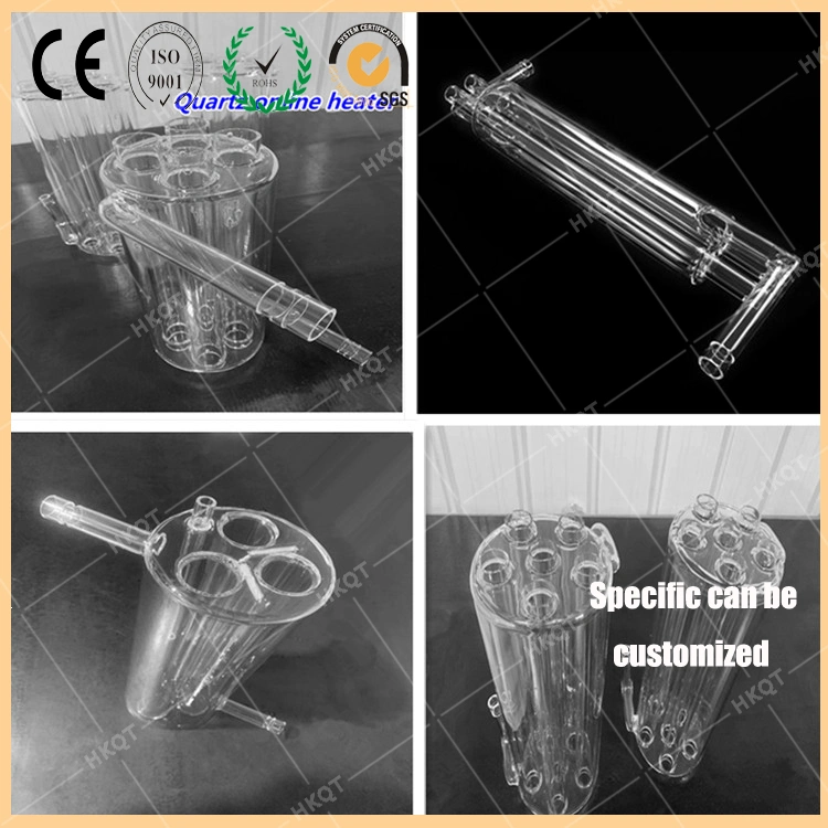
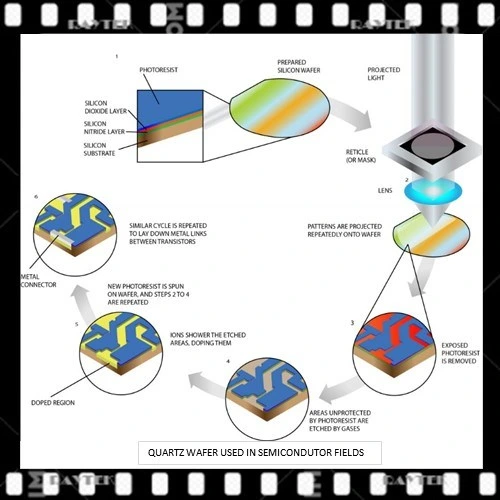
| Applying 1 | Laser systems/Laser optics |
| Applying 2 | All types of sensors and chips |
| Applying 3 | Optical windows and lens |
| Applying 4 | high frequency circuit / microwave circuit/Integrated circuit |
| Applying 5 | Internet of things array |
| Technical Data | Description & Value |
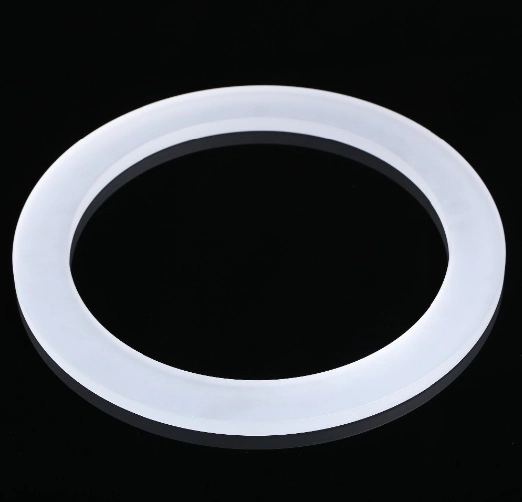
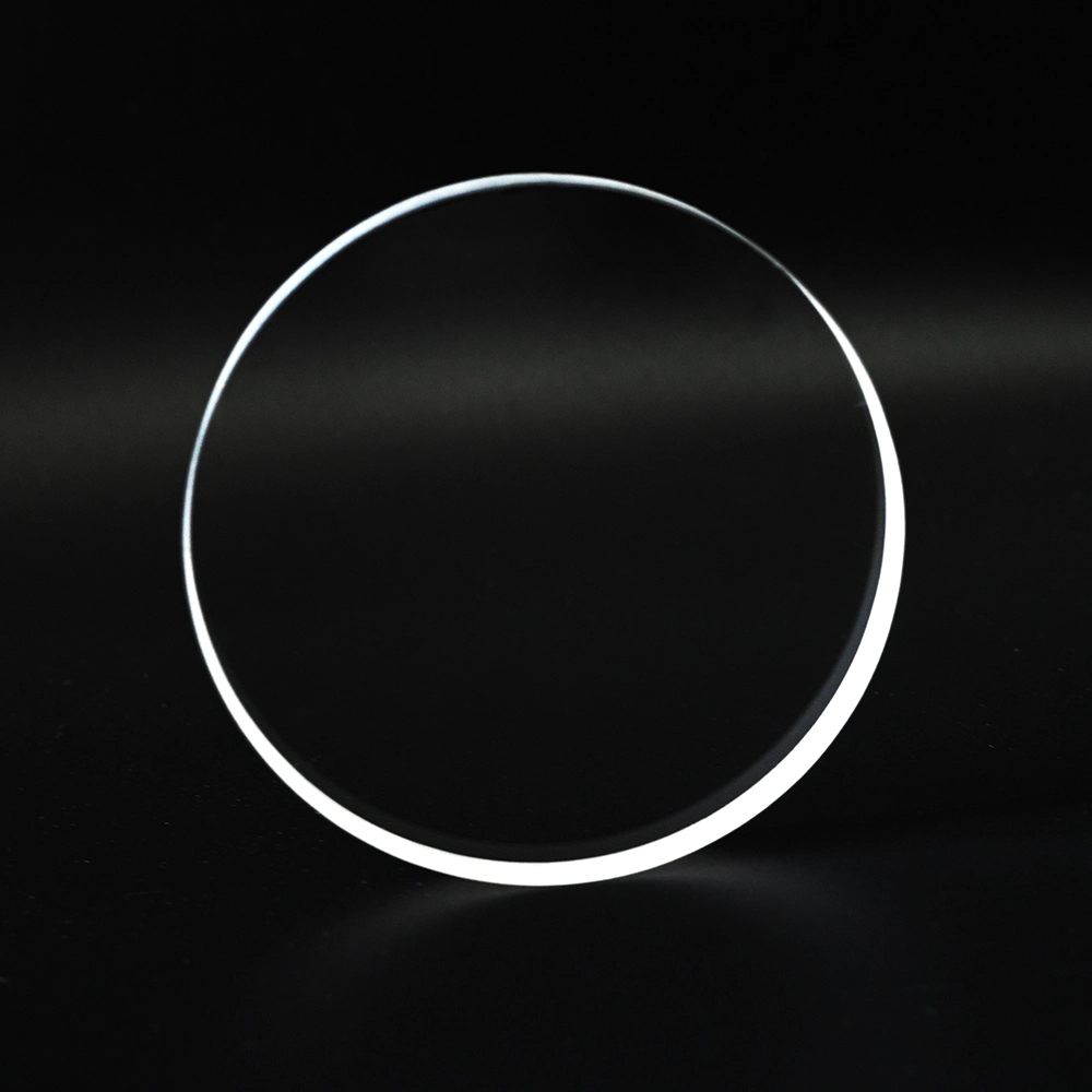
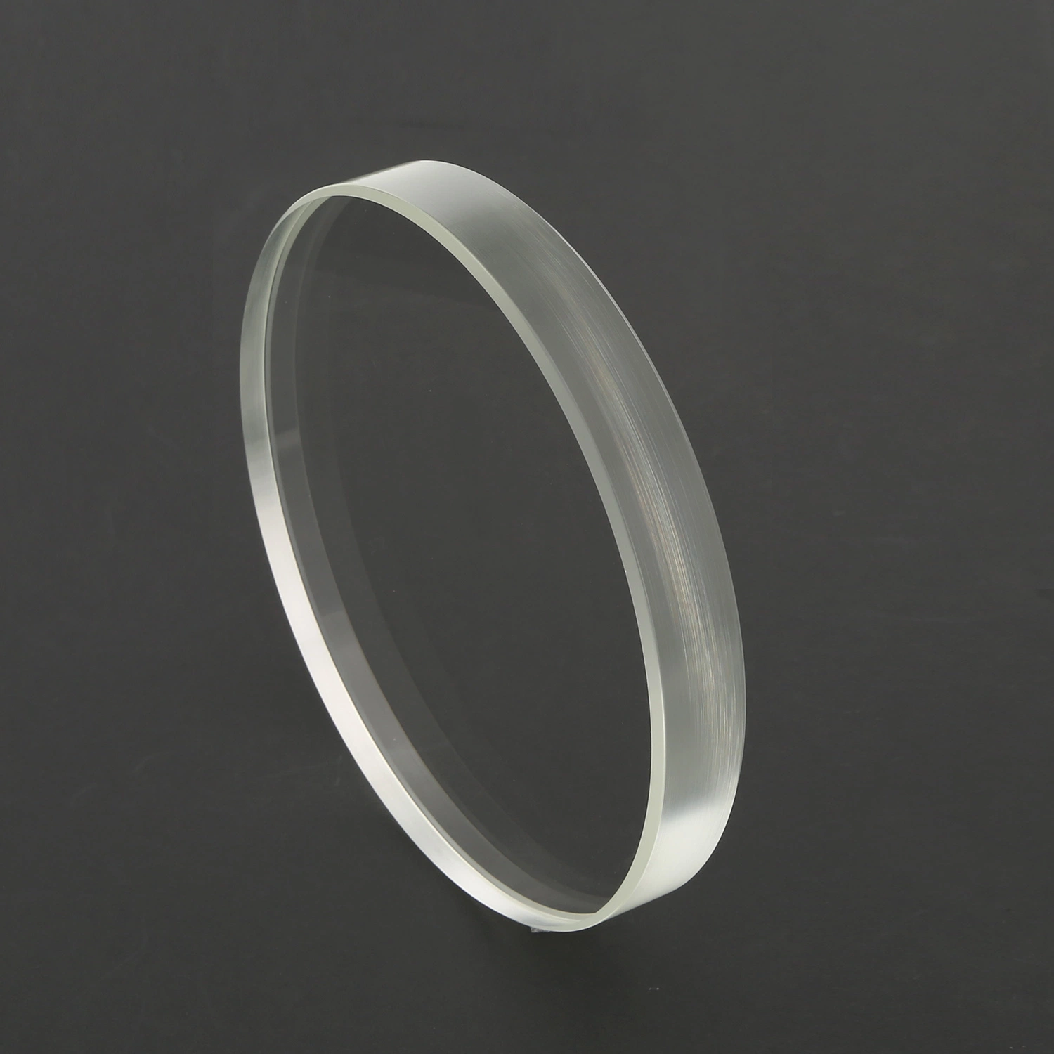
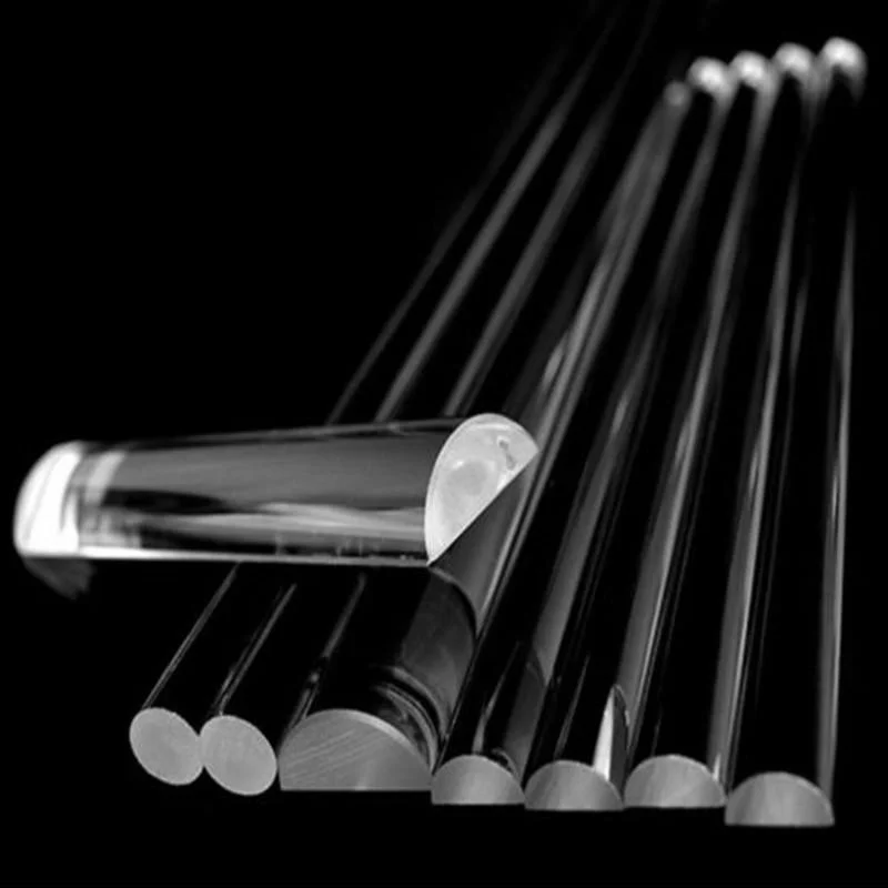
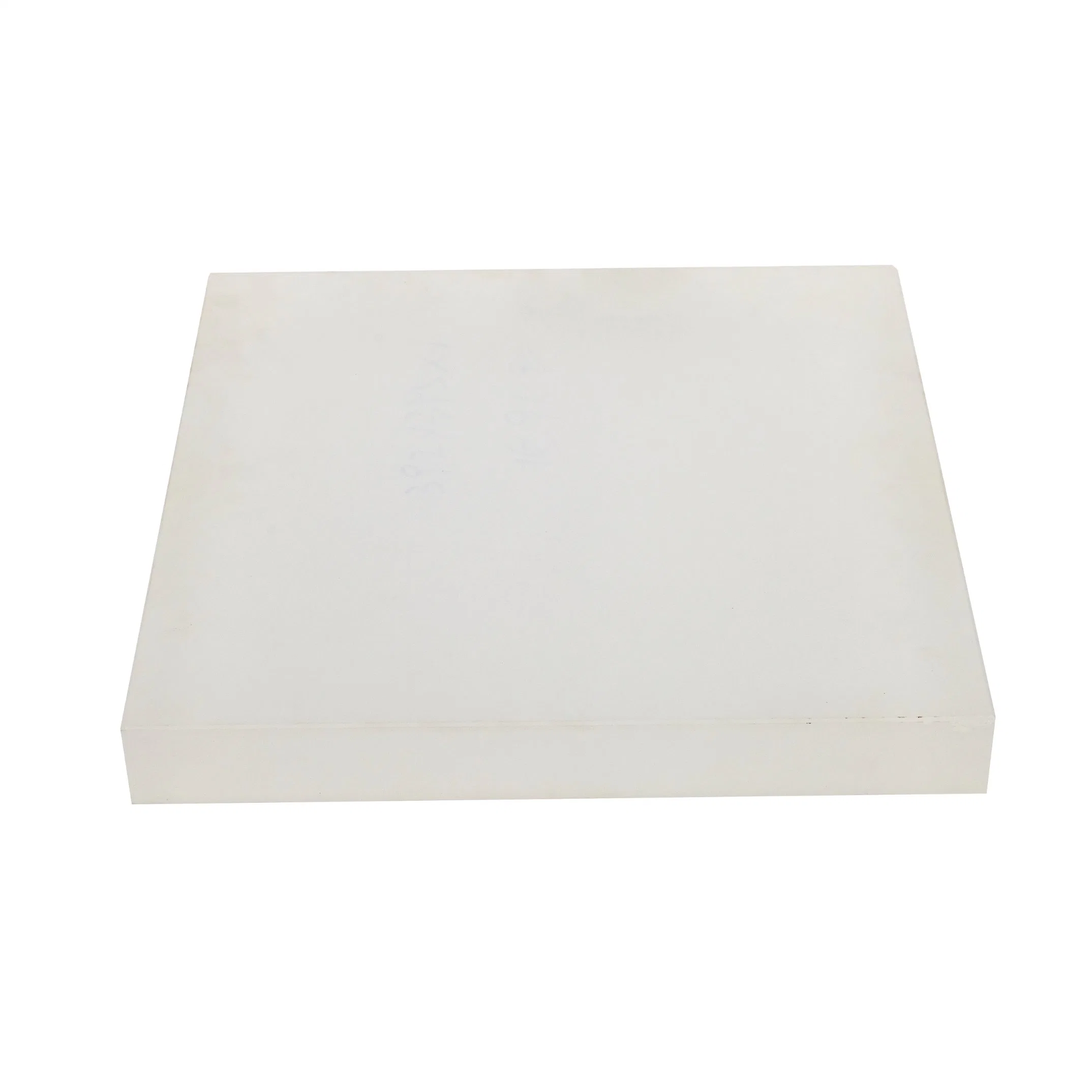
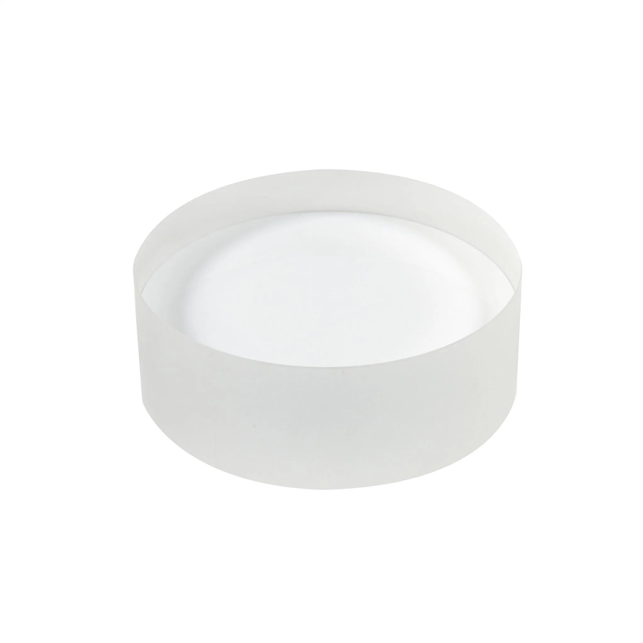
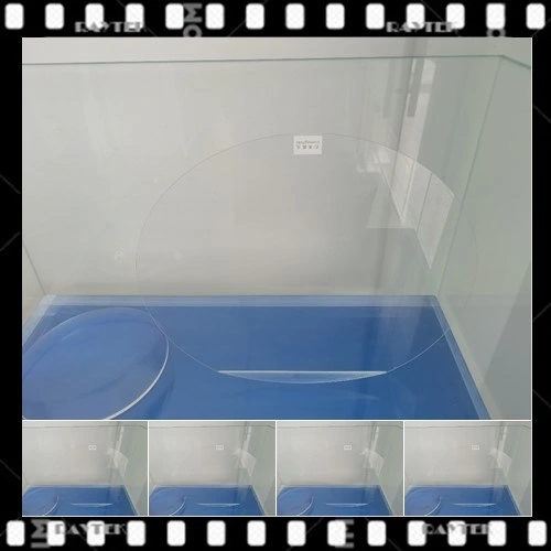
| Substrate | Corning 7980, Nikon, Heraeus etc quartz glass or fused silica quartz |
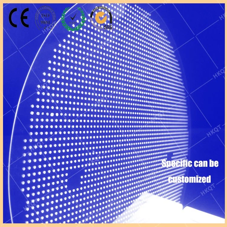
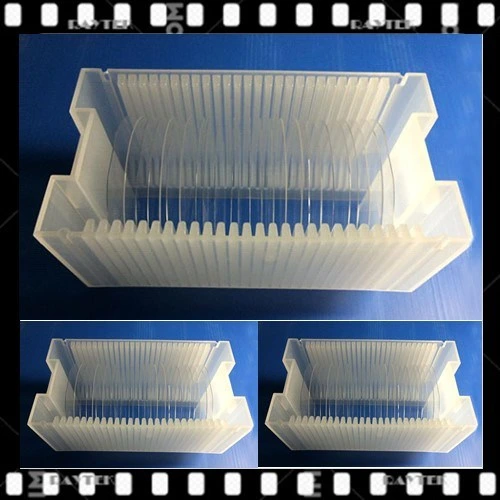
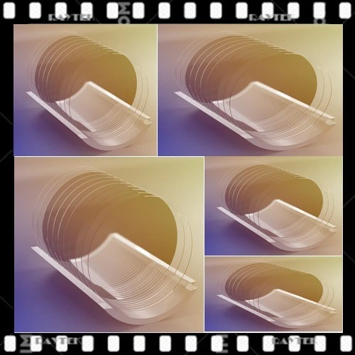
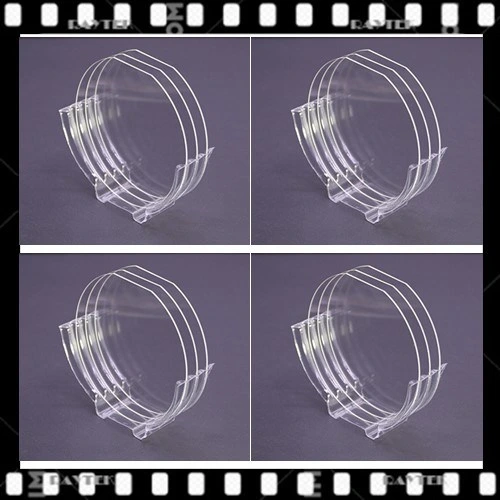
| Size | 2, 3, 4, 5, 6, 8, 10, 12 inches,etc or customize as per demand |
| Thickness | 0.5, 1, 2, 3, 4, 6,7,8mm ,or customize as per demand |
| Polishing Workcrafts | Single surface polishing or double -surface polishing |
| Thickness Variation(TTV) | <3um |
| PPV | <=20um |
| Purity of quartz wafer | 1). synthetic quartz wafer 99.999% 2). high purity quartz wafer 99.99% |
| Quartz Wafer Design | ODM/OEM available |
| Data | 4 inch | 5 inch | 6 inch | 8 inch | 12 inch |
| Diameter | 100 ± 0.1 mm | 125 ± 0.1 mm | 150 ± 0.1 mm | 200 ± 0.1 mm | 300± 0.1 mm |
| Thickness | 500 ± 5 um or Customize | 625 ± 5 um or Customize | 675 ± 5 um or Customize | 725 ± 5 um or Customize | 900± 5 um or Customize |
| Roughness | Ra ≤ 1 nm | Ra ≤ 1 nm | Ra ≤ 1 nm | Ra ≤ 1 nm | Ra ≤ 1 nm |
| Warpage | ≤ 10um | ≤ 10um | ≤ 10um | ≤ 10um | ≤ 10um |
| Planeness | ≤ 3 um | ≤ 3 um | ≤ 3 um | ≤ 3 um | ≤ 3 um |
| Surface Quality | 20/10 | 20/10 | 20/10 | 20/10 | 20/10 |
| Shape | Round, with locating edge and locating angle | ||||
| Chamfering | 45°, SEMI Spec; C Shape | ||||
| Substrate | Corning, Nikon, Heraeus etc. | ||||