 Complaint

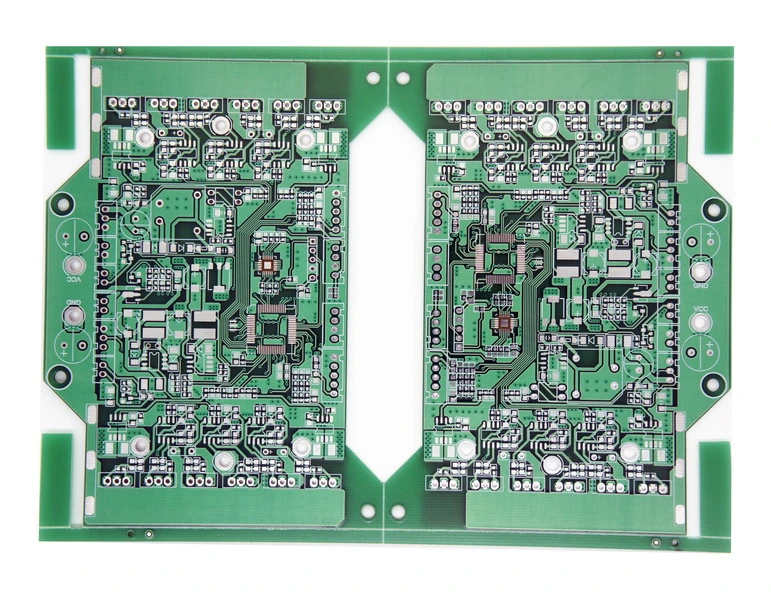
Specification: | ||||
PCB layers: | 1-24layers | |||
PCB materials: | CEM1, CEM3, Rogers, FR-4, High Tg FR-4, Aluminum Base, Halogen Free | |||
PCB max. board size: | 620*1100mm | |||
PCB certificate: | RoHS Directive-Compliant | |||
PCB Thickness: | 1.6 ±0.1mm | |||
Out Layer Copper Thickness: | 0.5-5oz | |||
Inner Layer Copper Thickness: | 0.5-4oz | |||
PCB max. board thickness: | 6.0mm | |||
Minimum Hole Size: | 0.20mm | |||
Minimum Line Width/Space: | 3/3mil | |||
Min. S/M Pitch: | 0.1mm(4mil) | |||
Plate Thickness and Aperture Ratio : | 30:1 | |||
Minimum Hole Copper: | 20µm | |||
Hole Dia. Tolerance(PTH): | ±0.075mm(3mil) | |||
Hole dia. Tolerance(NPTH): | ±0.05mm (2mil) | |||
Hole Position Deviation: | ±0.05mm (2mil) | |||
Outline Tolerance: | ±0.05mm (2mil) | |||
PCB surface finished: | HASL Leadfree,Immersion ENIG,Chem Tin,Flash Gold,OSP,Gold finger,Peelable,Immersion Silver | |||
PCB solder mask: | Black, white, yellow | |||
Legend: | White | |||
E-test: | 100% AOI, X-ray, Flying probe test. | |||
Outline: | Rout and Score/V-cut | |||
Inspection Standard: | IPC-A-610CCLASSII | |||
Certificates: | UL (E503048),ISO9001/ISO14001/IATF16949 | |||
Outgoing Reports: | Final Inspection, E-test, Solderability Test, Micro Section and More | |||
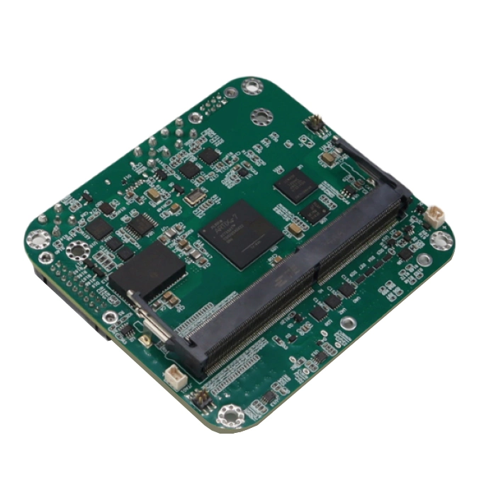
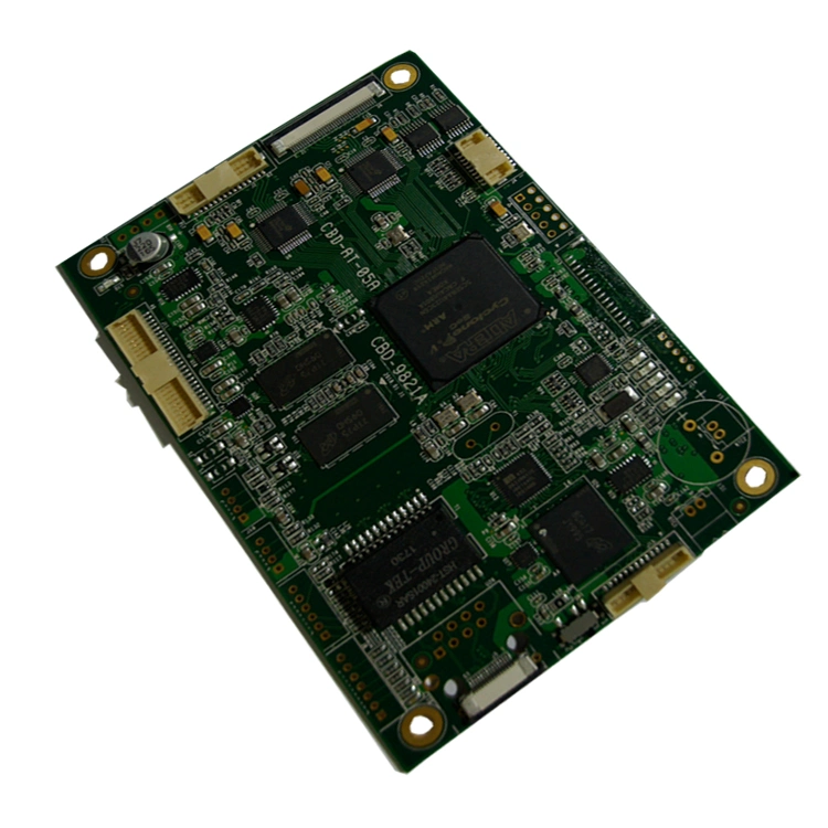
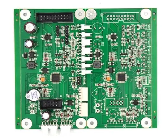
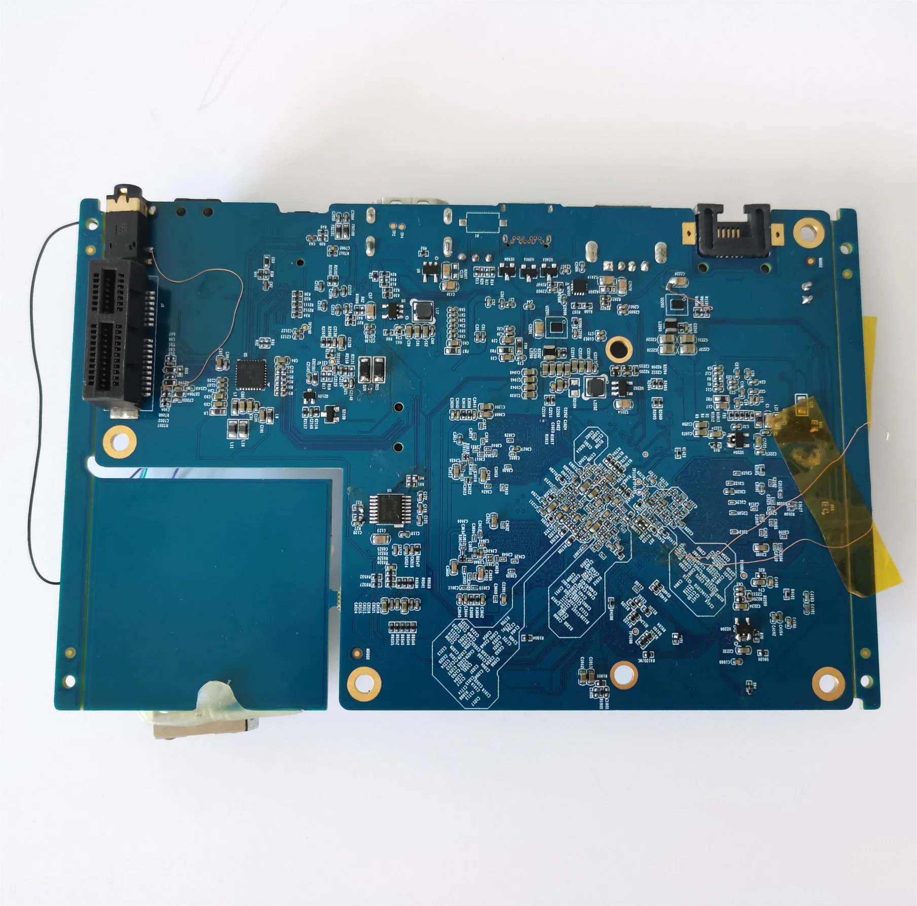
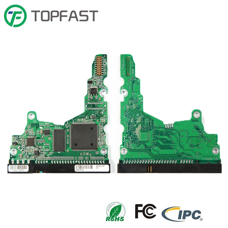
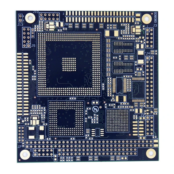
PCB Assembly OEM Service | ||||
Electronic Components Material Purchasing | ||||
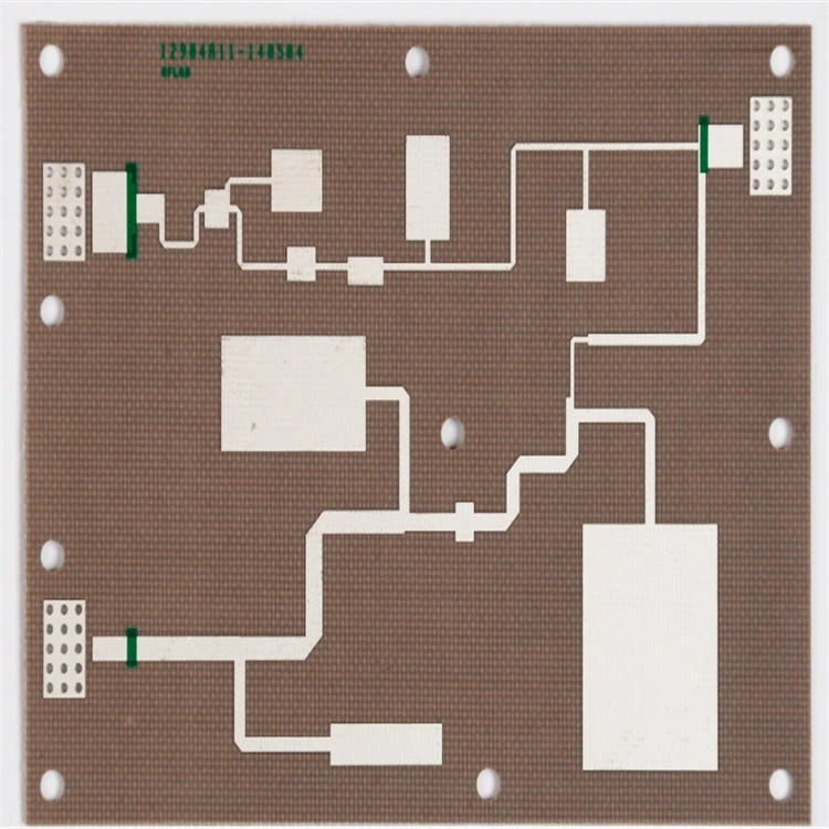
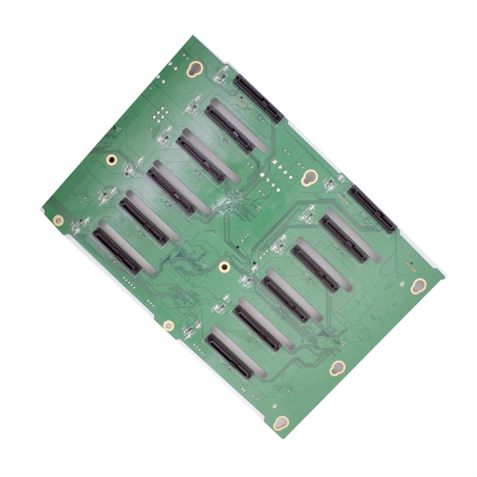
Bare PCB Fabrication | ||||
Cable, Wire-harness Assembly, Sheet Metal, Electrical Cabinet Assembly Service | ||||
PCB Assembly Service: SMT, BGA, DIP | ||||
PCBA test:AOI, In-Circuit Test (ICT), Functioal Test (FCT) | ||||
Conformal Coating Service | ||||
Prototyping and Mass Production |
PCBA ODM service | ||||
PCB Layout, PCBA Design According To Your Idea | ||||
PCBA Copy/Clone | ||||
Digital Circuit Design / Analog Circuit Design/ lRF Design /Embedded Software Design | ||||
Firmware and Microcode Programming Windows Application (GUI) Programming/Windows Device Driver (WDM) Programming | ||||
Embedded User Interface Design / lSystem Hardware Design |