
 Complaint

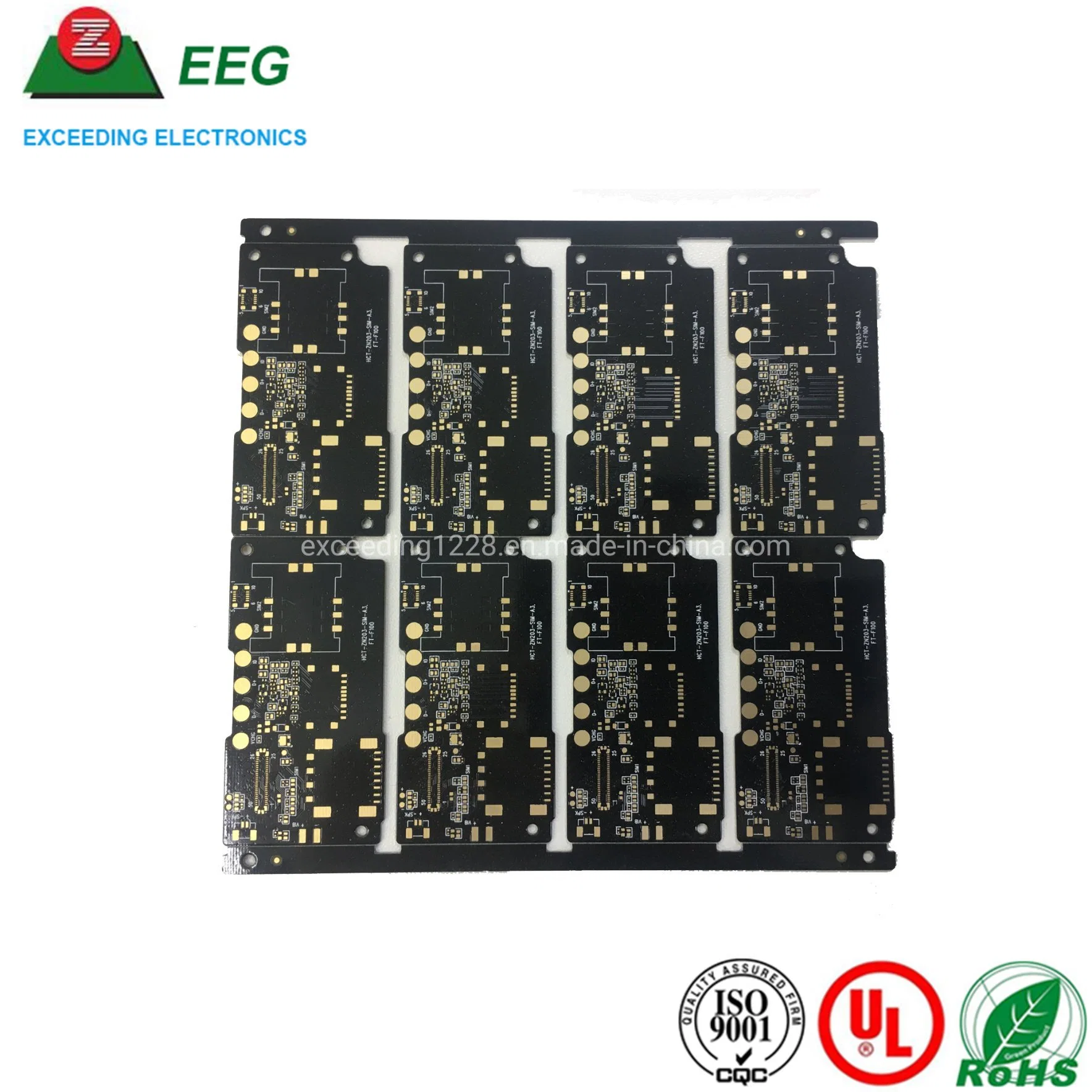
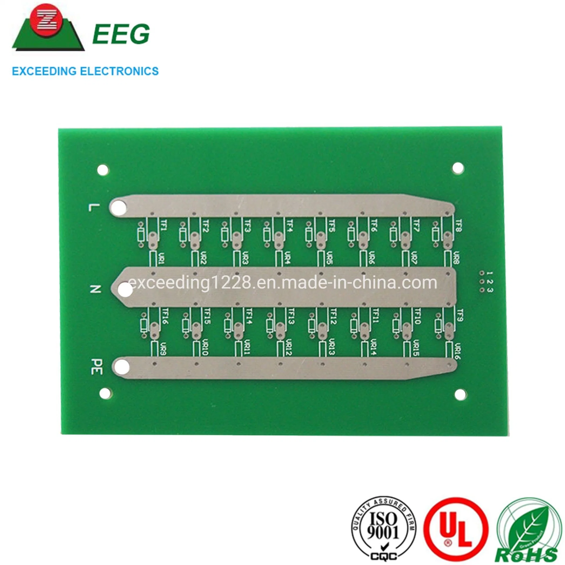
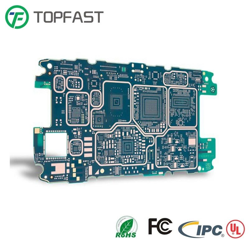
PCB Parameters
| Item | PCB Parameters |
| Material | FR4 (140Tg, 170Tg, 180Tg), FR-406, FR-408, 370HR, IT180A, Metal Core, Polyimide, Rogers 4350B/3003/4003C/5880, Taconic, Teflon, etc |
| Material Brands | KB, ITEQ, SY, ISOLA, Rogers (Arlon), Ventec, Laird, Nelco, Bergquist, DENKA, Panasonic, Taconic, or other laminate on customer's request |
| Layer Count | 1-40 |
| Flammaility | UL 94V-0 |
| Thermal Conductivity | 0.3W-300W/mk |
| Quality Standards | IPC Classes 2/3 |
| HDI Build-up | Any Layer, up to 3+N+3 |
| Board Thickness | 0.2~7mm |
| Min Thickness | 2-layer: 0.2mm 4-layer: 0.4mm 6-layer: 0.6mm 8-layer: 0.8mm 10-layer: 1mm More than 10 layers: 0.5*Layer Count*0.2mm |
| Copper Thickness | 0.5-20oz |
| Inks | Super White Inks/Solar/Carbon Inks |
| Solder Mask Thickness | 0.2mil-1.6mil |
| Surface Finishes | Bare Copper, Hasl lead-free, ENIG, ENEPIG, Gold Fingers, OSP, IAg, ISn, etc |
| Plating Thickness | HASL: Copper Thickness: 20-35um Tin: 5-20 um Immersion Gold: Nickel: 100u"-200u" Gold: 2u" -4u" Hard Plated Gold: Nickel: 100u"-200u" Gold: 4u"-8u" Golden Finger: Nickel: 100u"-200u" Gold: 5u"-15u" Immersion Silver: 6u"-12u" OSP: Film 8u"-20u" |
| Min Hole Size | 0.15mm |
| Min Trace Width/Spacing | 2mil/2mil |
| Via Plugging | 0.2~0.8mm |
| Line Width/Space Tolerance | ±10% |
| Board Thickness Tolerance | ±5% |
| Hole Diameter Tolerance | ±0.05mm |
| Hole Location Tolerance | ±2mil |
| Layer to Layer Registration | 2mil |
| S/M Registration | 1mil |
| Aspect Ratio | 10:01 |
| Blind Vias Aspect Ratio | 1:01 |
| Outline Tolerance | ±0.1mm |
| V- CUT Tolerance | ±10mi |
| Bevel Edge | ± 5mil |
| Warp and Twist | ≤0.50% (max cap) |
| Quality Test | AOI, 100% E-test |
| Value-Added Services | DFM Check, Expedited Production |
| Featured Processes | Bonding, Impedance Control, Via in Pad, Press Fit Hole, Countersink/Counterbore Hole, Castellated Vias, Edge Plating, Peelable Solder Mask, Resin Plugged, Plating Flat |
| Data Formats | Gerber, DXF, PCBdoc, ODB++, HPGL, BRD, etc |
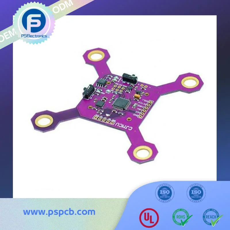
PCBA Abilities
| Item | PCBA Abilities |
| Turnkey Service | PCB Design + PCB FAB + Components Sourcing + PCB Assembly + Package |
| Value-Added Services | BOM Analysis, Conformal Coating, IC Programming, Wire Harness & Cable Assembly, Box Building |
| Assembly Details | 5 SMT + 2 DIP (Dust and anti-static lines) |
| Assembly Abilities | SMT 5 million points per day DIP 10 thousands pieces per day |
| Technical Support | Free DFM/A check, BOM analysis |
| Handing Standards | IPC-A-600H, IPC-A-610F, J-STD-001F |
| MOQ | 1 piece |
| Inspection & Testing | Visual Inspection, AOI, SPI, X-ray inspection. First article inspection for each process. |
| IQC + IPQC + FQC + OQC Inspection Flow | |
| Flying probe test/In-circuit test/Function test/Burn-in test | |
| Files We Need | PCB: Gerber (CAM, PCB, PCBDOC) |
| Components: Bill of Material (BOM list) | |
| Assembly: Pick-and-Place file | |
| Functional test: Test Guide | |
| PCB Panel Size | Min: 0.25×0.25 inches (6×6mm) |
| Max: 20×20 inches (500×500mm) | |
| PCB Solder Type | Water soluble solder paste, RoHS lead-free |
| PCB Assemble Methods | SMT, THT & Hybrid, single or double side placement, Part removal and replacement. |
| Components Details | Passive down to 0201 (01005) size |
| Press fit connectors | |
| QFP/BGA/LGA/QFN/COB/COF | |
| CSP/WLCSP/POP | |
| Fine Pitch High Pin Count Connectors | |
| BGA repair and reball | |
| Lead Time | Prototype: 5-15 working days; Mass production: 20~25 working days. The fastest delivery time is 3 days. |
| Packaging | Anti-Static Bags/Customized Packaging |
Main Customers
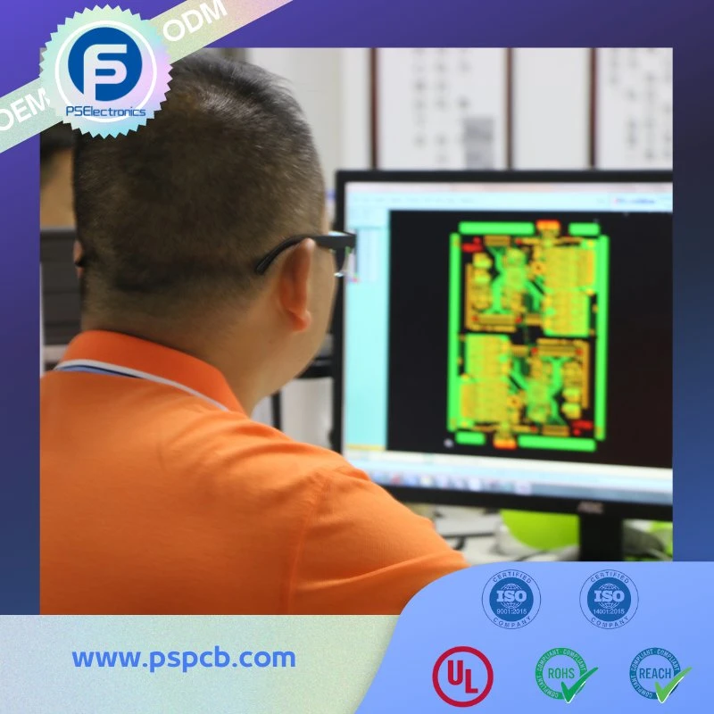
Process
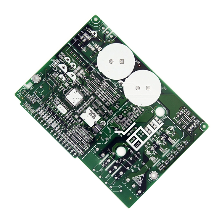
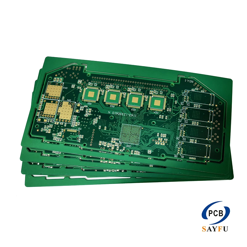
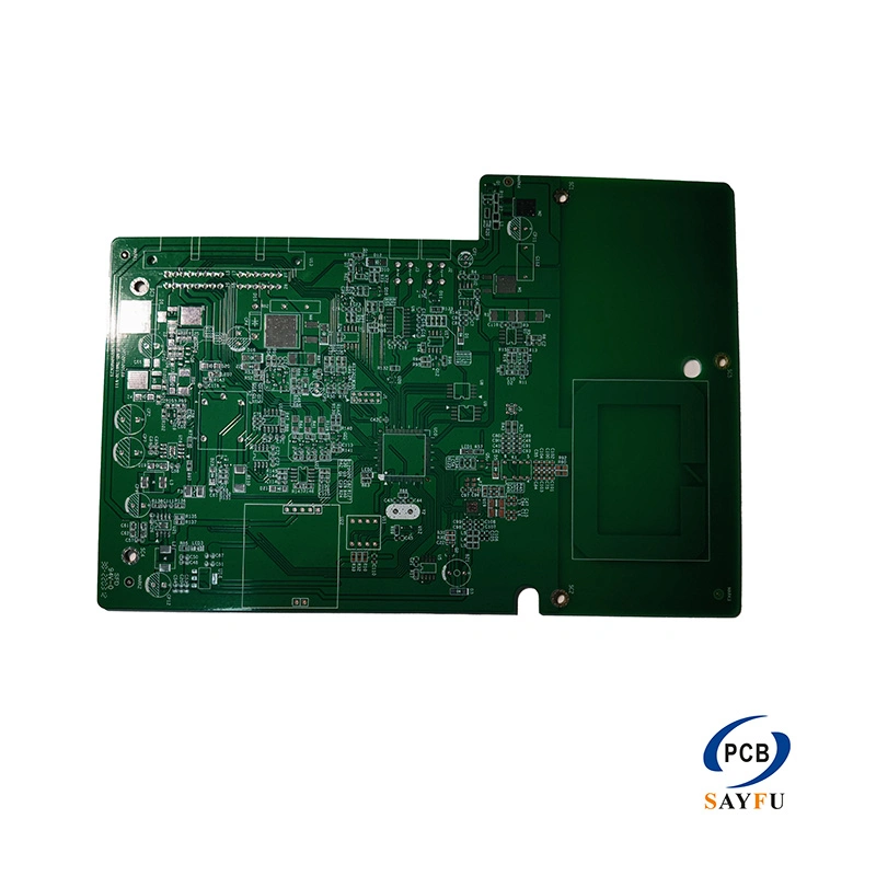
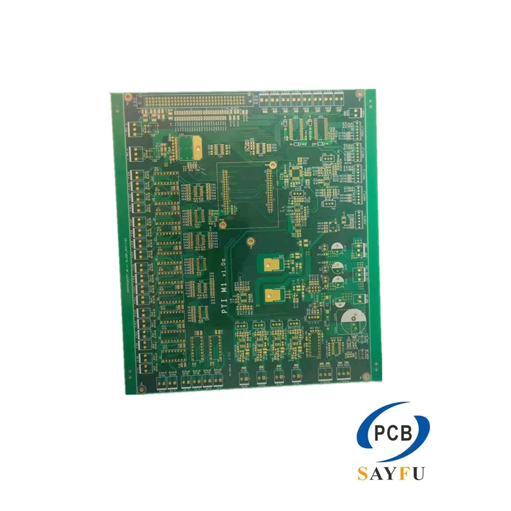
PCBA Showcase
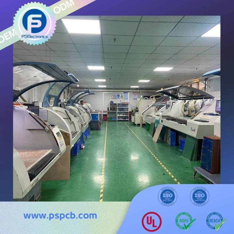
SMT & DIP Workshop
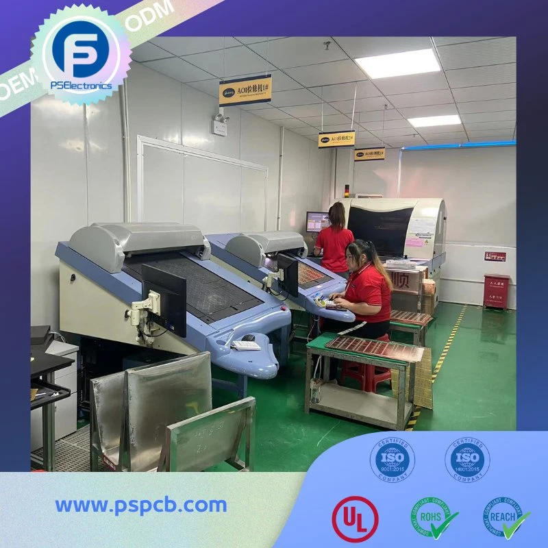
Test and Maintenance Workshop
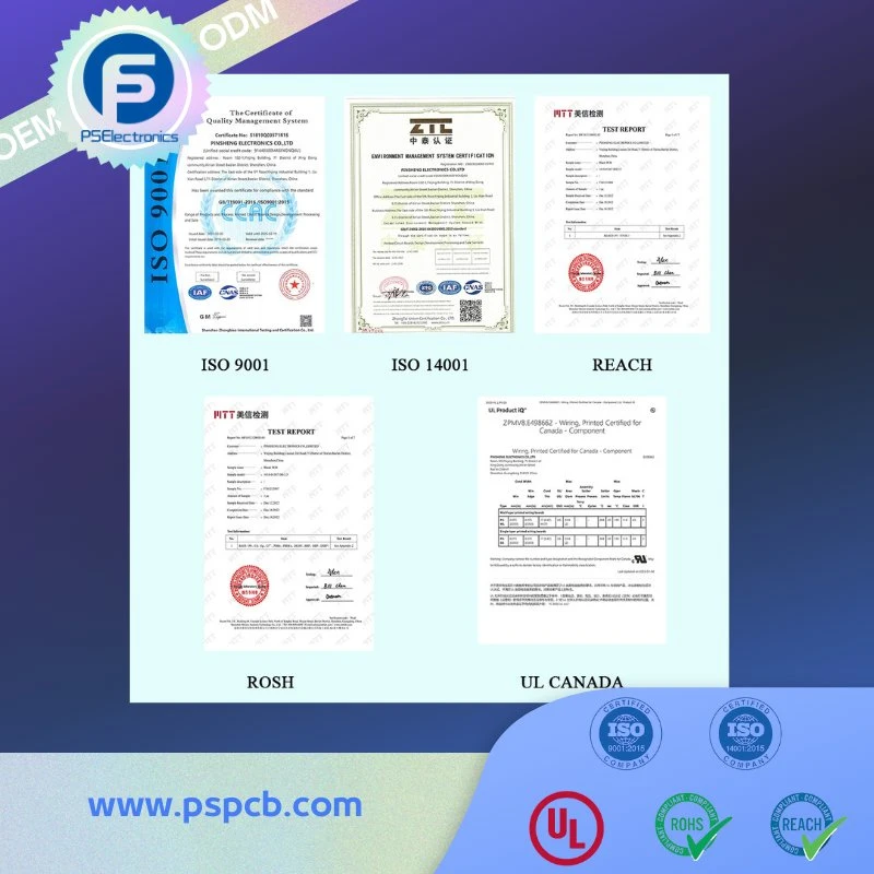
CERTIFICATIONS
FAQ
Q1: What's your monthly capacity of PCB assembly