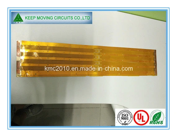
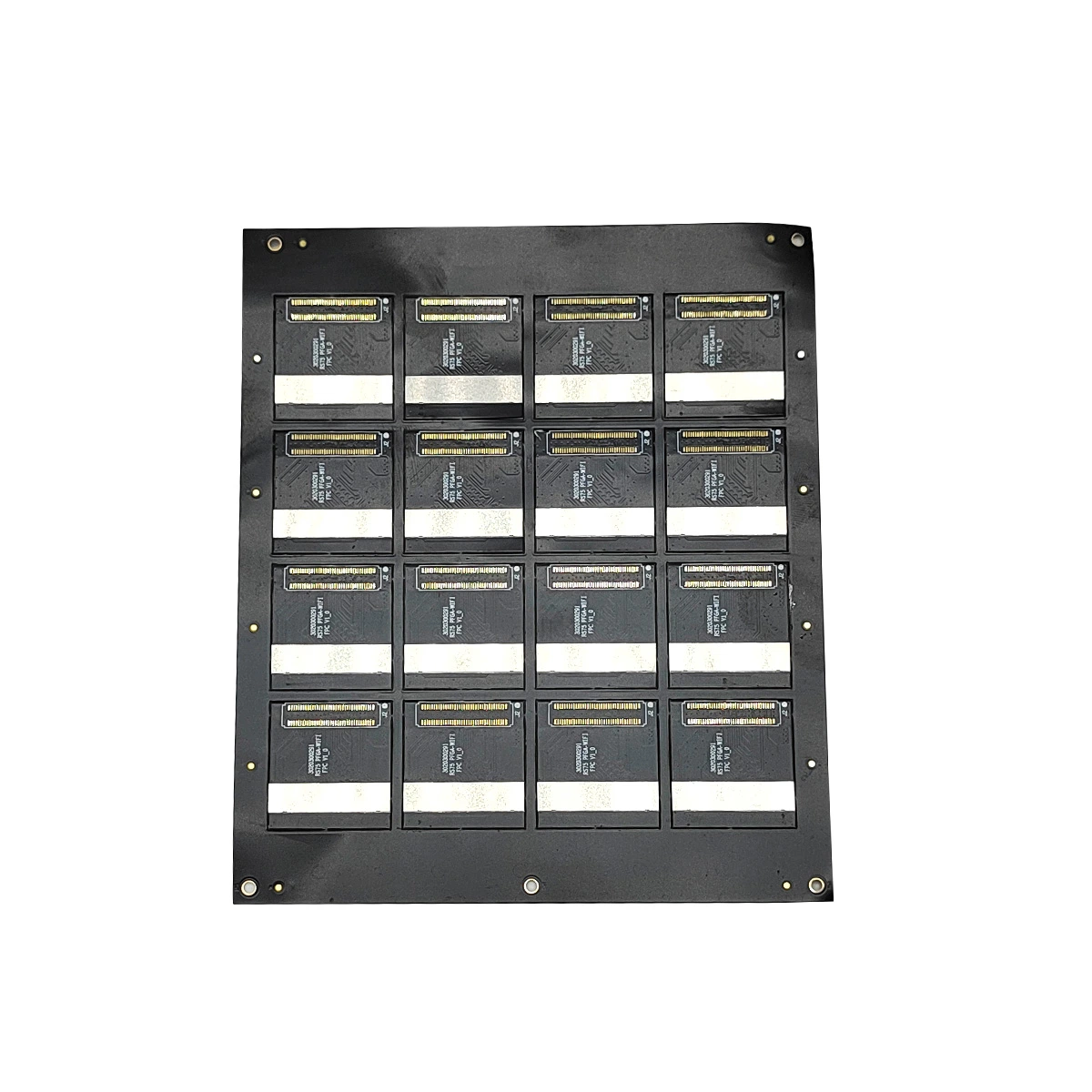
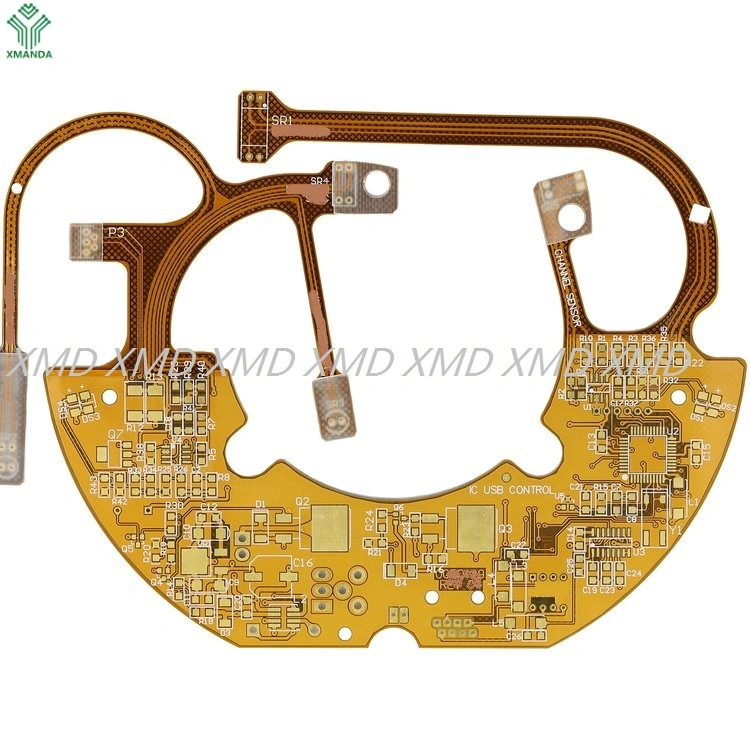
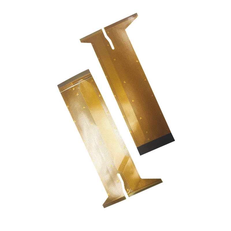
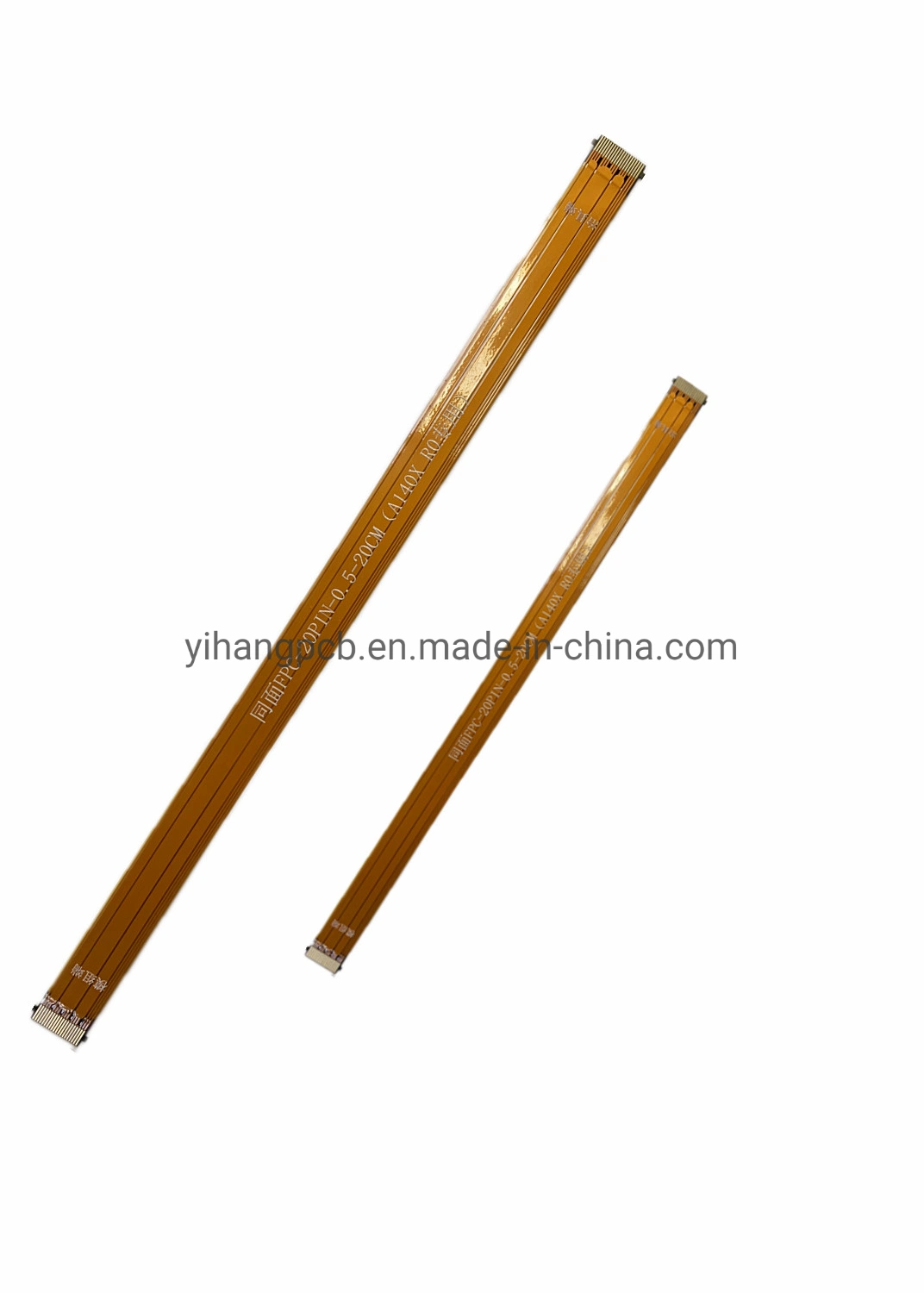
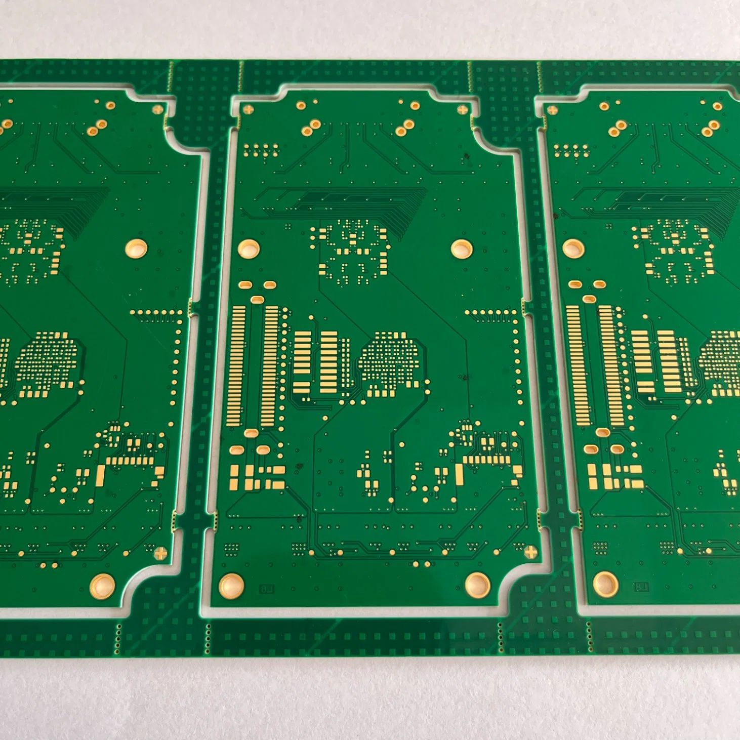
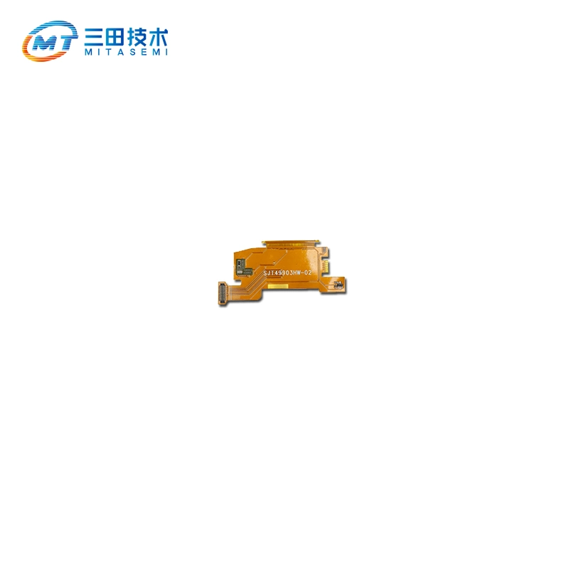
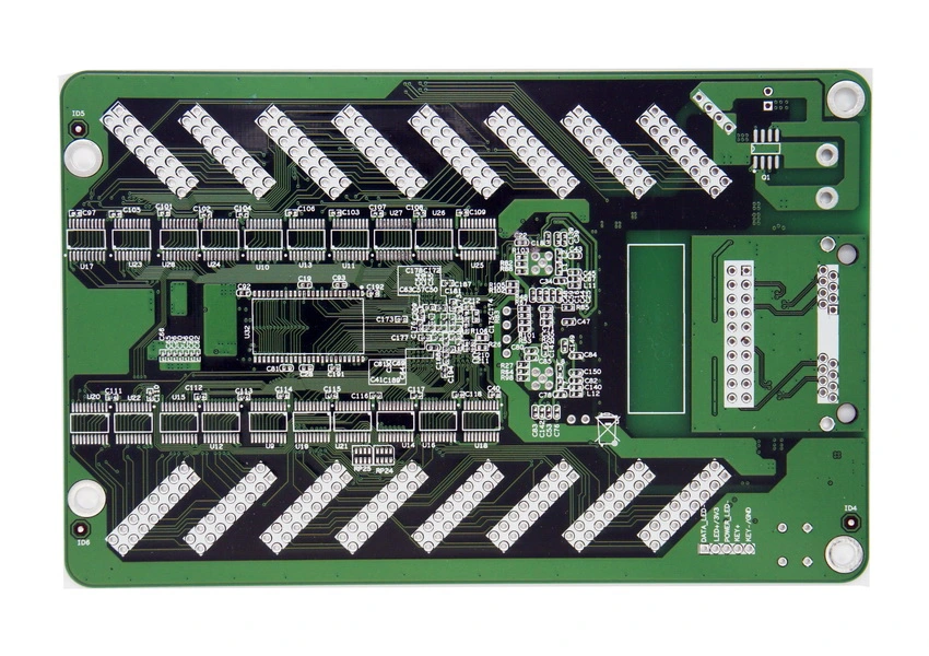
Description
WELCOME TO XJY--------------
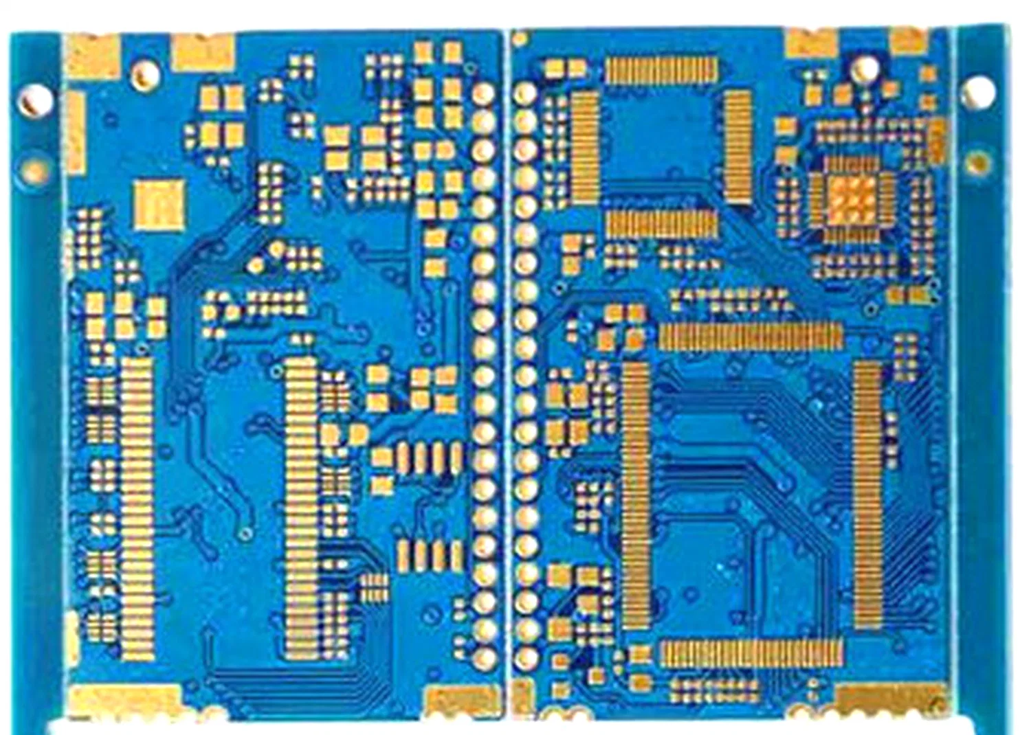
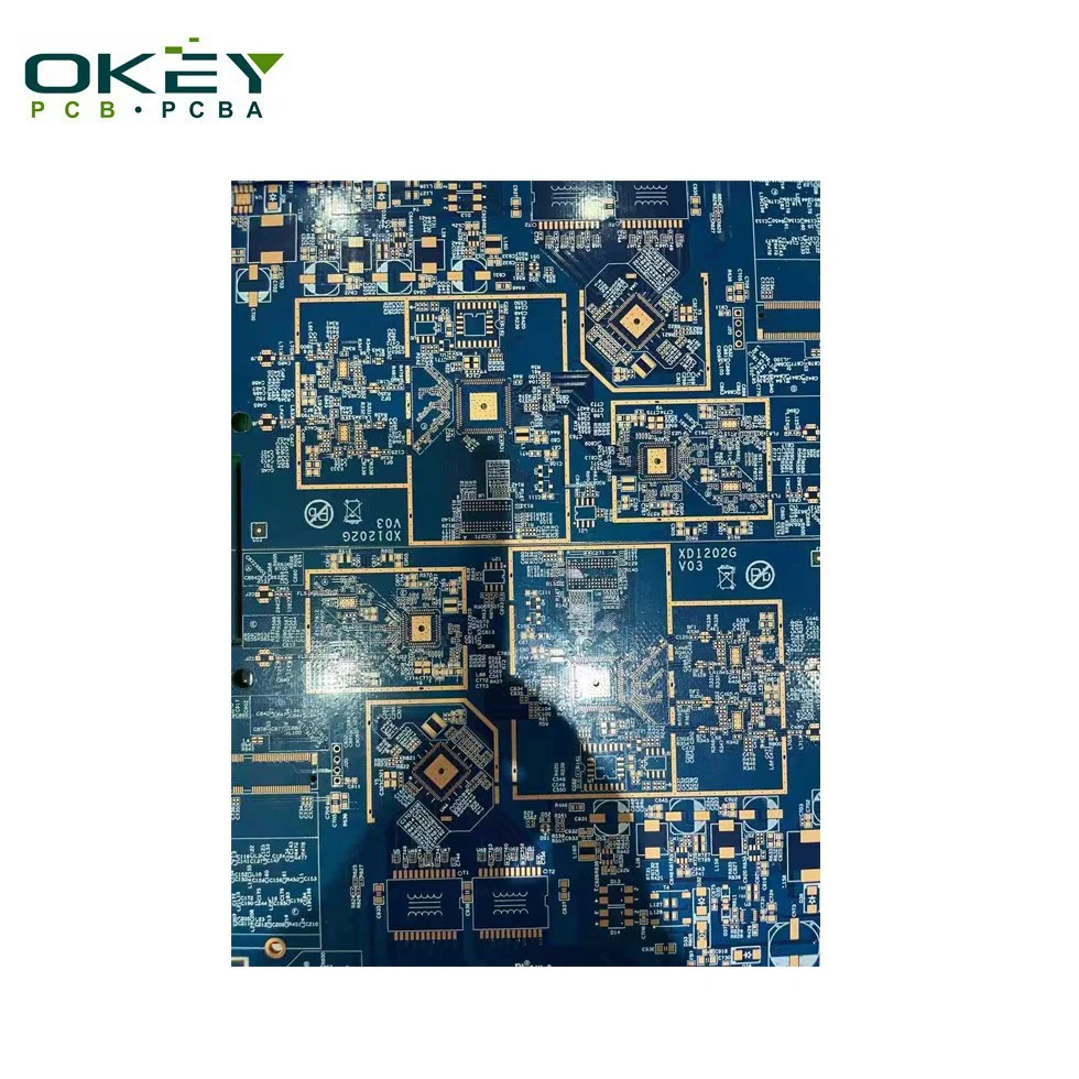
Shenzhen Xinjiaye Electronics Technology Co., Ltd is a professional pcb manufacturer has over 10 years experience. We are able to offer 1 to 24 Layer PCB, ranging from pcb produce, components purchase, pcb assembly, pcb copy service.Our products are widely used in communication apparatus, automobile electronics, auto parts, computers, medical devices, light systems, outdoor systems, network devices and consumer electronics class fields.
+++++++
Quick Details
Place of Origin: |
Shenzhen (Mainland) |
Brand Name: |
XJY |
Model Number: |
xjy-pcb 279 |
Number of Layers: |
2-32 |
Base Material: |
FR-4, others |
Copper Thickness: |
1oz-5oz |
Board Thickness: |
1mm |
Min. Hole Size: |
0.6mm |
Min. Line Width: |
4mil |
Min. Line Spacing: |
4mil |
Surface Finishing: |
HAL,Immersion gold, Immersion silver |
certificate: |
ISO9001, ISO14001,TS16949, UL certifications |
solder mask color: |
green,red,blue,yellow,white |
shipping term: |
by FEDEX/DHL/EMS/TNT/UPS |
Payment: |
T/T,Western Union,Paypal |
MOQ: |
1 Piece |
Delivery: |
2-15 days after your payment |
Packaging: |
vacuum packing, anti-static package |
++++++
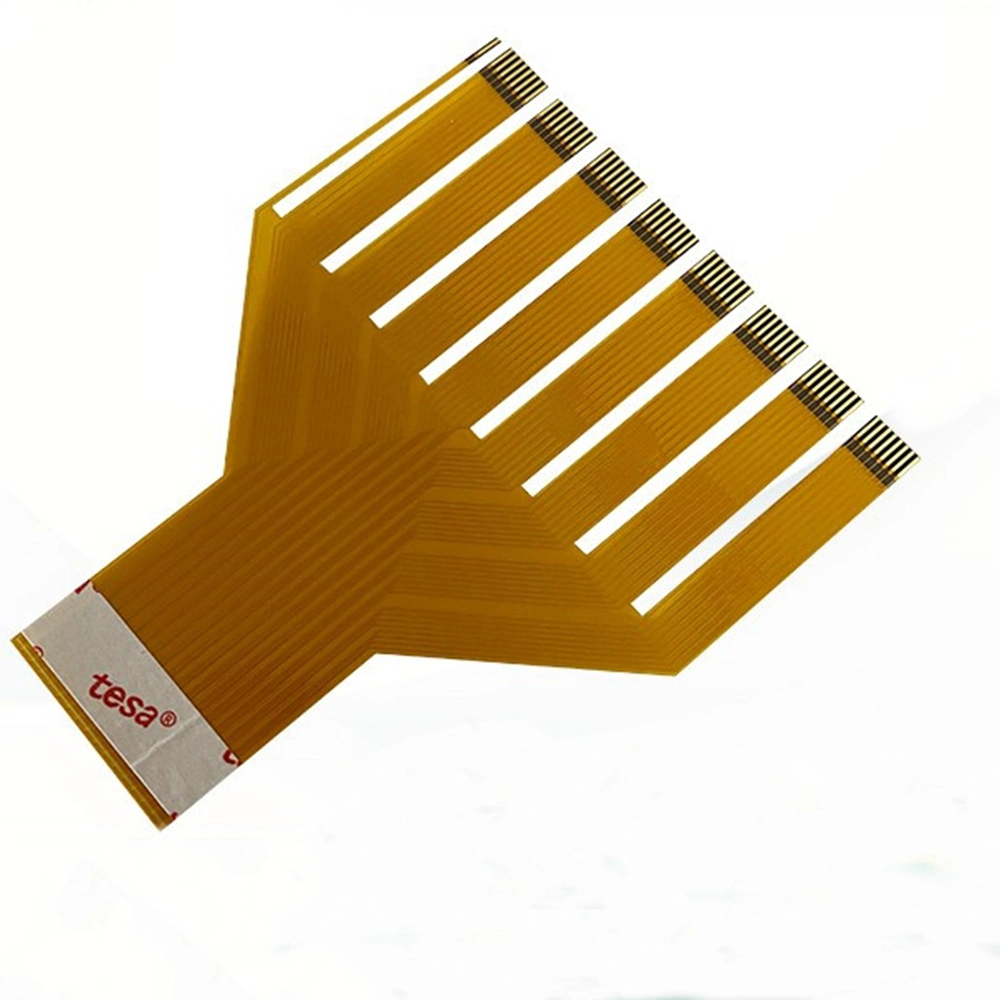
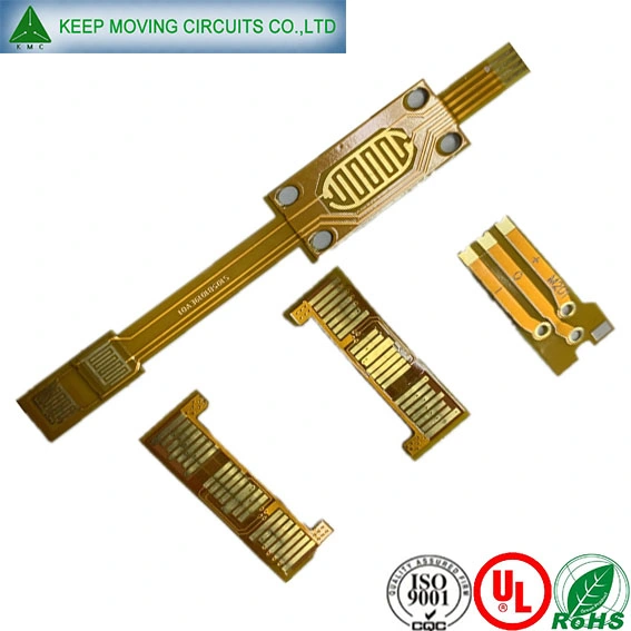
+++++++Technology capability
| Items | Single/Double-sided Board/Multilayer Board/FPC(1-24Layer) |
| Base Materials | FR-4(High TG 150°-170°),FR1,Aluminum,CEM-3,BT,94vo |
| Finish copper thickness | Outer 6 OZ,Inner 4 OZ |
| Surface finish | ENIG, ImAg, ImSn, OSP, HASL,Plating gold |
| Finished Board Size | Max Double-sided Board | 640mm χ 1100mm |
| Max Multilayer Board | 640mm χ 1100mm |
| Finished Board Hole Size (PTH Hole) | Min Finished Board Hole Size | 0.15mm |
| Conductor Width and Spacing | Min Conductor Width | 0.01mm |
| Min Conductor Spacing | 0.01mm |
| Thickness of Plating and Coating Layer | PTH Wall Copper Thickness | >0.02mm |
| Tin Solder Thickness ( Hot Air Leveling ) | >0.02mm |
| Nickl/Gold Thickness | For customer special need |
| Nickl Plating Layer | >2um |
| Gold Plating Layer | >0.3um |
| Bare Board Test | Single Side Test | Max Test Point | 20480 |
| Max Board Test Size | 400mm χ 300mm |
| Double Side Test | Max Test Point | 40960(General Use) |
| 4096(Special Use) |
| Max Board Test Size | 406mm χ 325mm |
| 320mm χ 400mm |
| Min Test pitch of SMT | 0.5mm |
| Test Voltage | 10-250V |
| Mechanical Process | Chamfer | 20°, 30°, 45°, 60° |
| Angle Tolerance | ± 5° |
| Deepness Tolerance | ± 0.20mm |
| V-Cut Angle | 20°, 30°, 45° |
| Board Thickness | 0.1-3.2mm |
| Residues Thickness | ± 0.025mm |
| Cell Paraposition Precision | ± 0.025mm |
| Tolerance of Out-shape Process | ± 0.1mm |
| Board Warp | Max Value | 0.7% |
| Optical Plotting | Max Plotting Area | 66mm χ 558.8mm |
| Precision | ± 0.01mm |
| Repetitive Precision | ± 0.005mm
|
Our PCB board manufacture
* PCB board file with parts list provided by customers
* PCB board made, circuit board parts purchased by us
* Electronic testing circuit board
* Fast delivery, anti-static package
* RoHS Directive-compliant, lead-fre
Testing Procedures For PCB Board
---We perform multiple quality assuring procedures before shipping out
any PCB board. These include:
* Visual Inspection
* Flying probe
* Bed of nails
· * Impedance control
· * Solder-ability detection
* Digital metallograghic microscope
· *AOI (Automated Optical Inspection)
Detailed Terms for PCB Manufacturing
---Technical requirement for PCB assembly:
* Professional Surface-mounting and Through-hole soldering Technology
* Various sizes like 1206, 0805, 0603 components SMT technology
* ICT(In Circuit Test), FCT(Functional Circuit Test) technology.
* PCB Assembly With UL, CE, FCC, RoHS Approval
* Nitrogen gas reflow soldering technology for SMT.
* High Standard SMT&Solder Assembly Line
* High density interconnected board placement technology capacity.
Delivery Time for PCB board
1) PCB production time: Sample: 3-4 days / mass production: Within 7 days
2) Component purchase: 2 days if all components is available in our domestic market.
3) PCB Assembly: Samples: Whthin 2 days / mass production: Within 5 days
Quotation Requirement:
Following specifications are needed for quotation:
A) Base material:
B) Board thickness:
C) Copper thickness
D) Surface treatment:
E) color of solder mask and silkscreen:
F) Quantity
Shipping Method and Payment terms:
1. By DHL, UPS, FedEx, TNT using clients account.
2. We suggest you using our DHL, UPS, FedEx, TNT forwarder.
3. By EMS (Usually for Russia Clients), price is high.
4. By sea for mass quantity according to customer's requirement.
5. By customer's Forwarder
6. By Paypal, T/T, West Union, etc.
Other Service:
A) We have many special material as rogers, teflon, taconic, Fr-4 high tg, Ceramic in stock. Welcome to send us your inquiry.
B) We also provide sourcing components, PCB design, PCB copy, PCB drawing, PCB assembly and so on.so provide sourcing components, PCB design, PCB copy, PCB drawing, PCB assembly and so on.
If you have any question,please feel free to contact me!
 Complaint